


 EMERGING TECH
EMERGING TECH
EMERGING TECH
EMERGING TECH
Intel Corp. held its annual Architecture Day semiconductor event today, where executives shared technical details about several upcoming chips for the data center and consumer markets.
One of the main highlights from the event is Alder Lake. It’s an upcoming central processing unit for personal computers that will feature not one type of processing core as is the usual practice, but two. Intel also shared new details about its ambitious Ponte Vecchio artificial intelligence chip for data centers. Ponte Vecchio, described as the company’s most complex system-on-chip to date, features a hefty 100 billion transistors arranged in an unconventional three-dimensional structure.
The Alder Lake processor line for Windows desktops and laptops represents a significant departure from Intel’s earlier CPUs. A typical Intel CPU comprises multiple processor cores that all have the same design, meaning they have identical performance and specifications. Alder Lake processors, in contrast, will feature two sets of cores, each of which is based on a separate design. Intel calls them Performance cores and Efficiency cores.
Alder Lake processors will assign the most demanding computing tasks to Performance cores, which as their name suggests are optimized for speed. The Efficiency cores provide less computing power and consume a lower amount of electricity.
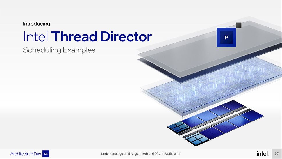
The task of determining how computations should be split among the Performance and Efficiency cores will be managed by a new mechanism dubbed the Intel Thread Director. The mechanism can help Windows computer, particularly laptops, save power by running the least demanding processing tasks on Efficiency cores and benefit from the cores’ lower electricity usage.
Intel Thread Director isn’t the only feature that will make Alder Lake a more compelling choice for computer makers than earlier Intel chips.
The CPU series’ Performance cores are about 19% faster than Intel’s current-generation Cypress Cove core when operating at the frequency. The Performance cores run AI models particularly quickly thanks to a new module optimized for matrix multiplications, the mathematical operations used by AI models to analyze data. The module performs matrix multiplications nearly eight times faster than earlier Intel silicon.
The Efficiency cores, the other element of the Alder Lake architecture, bring improvements as well. Intel says that they can match the single-threaded performance of its popular Skylake core design while using just 40% of the power.
Intel is looking to take on Nvidia Corp. in the AI silicon market with Ponte Vecchio, which the company describes as its most complex system-on-chip or SOC to date. Ponte Vecchio features some 100 billion transistors, nearly twice as many as Nvidia’s flagship A100 data center graphics processing unit.
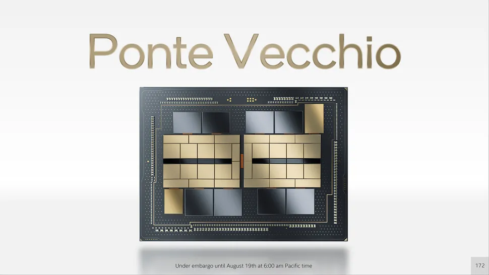
The chip’s 100 billion transistors are divided among no fewer than 47 individual processing modules made using five different manufacturing processes. Normally, an SOC’s processing modules are arranged side by side in a flat two-dimensional design. Ponte Vecchio, however, stacks the modules on one another in a vertical, three-dimensional structure created using Intel’s Foveros technology.
The bulk of Ponte Vecchio’s processing power comes from a set of modules aptly called the Compute Tiles. Each Compute Tile has eight Xe cores, GPU cores specifically optimized to run AI workloads. Every Xe core, in turn, consists of eight vector engines and eight matrix engines, processing modules specifically built to run the narrow set of mathematical operations that AI models use to turn data into insights.
The Compute Tiles are complemented by Xe Link Tiles, which allow the chip to connect to other Ponte Vecchio SOCs in order to coordinate processing. Large-scale AI models often distribute processing tasks across multiple chips. It’s therefore essential to have a mechanism that can manage the task of orchestrating the chips’ computations.
The Compute Tiles and Xe Link Tiles in Ponte Vecchio both sit on a Base Tile that functions as the chip’s foundation. Additionally, it contains auxiliary components such as memory modules for storing the data being processed.
Intel shared early performance data about the chip in conjunction with the release of the technical details. According to the company, early Ponte Vecchio silicon has demonstrated performance of more than 45 teraflops, or about 45 trillion operations per second. The chip achieved such speeds while processing FP32 floating point values, large numbers that take up 32 bits of storage space and are the basic unit of data used by many AI applications.
At least one customer has already signed up to use Ponte Vecchio. The Argonne National Laboratory will include Ponte Vecchio chips in its upcoming $500 million Aurora supercomputer. Aurora will provide one exaflop of performance when it becomes fully operational, the equivalent of a quintillion calculations per second.
Alongside the Alder Lake and Ponte Vecchio announcements, Intel shared new details about a number of upcoming chips today, most notably the next iteration of its Xeon server processor line.
The upcoming Xeon processors, codenamed Sapphire Rapids, will be made with the company’s seven-nanometer manufacturing process. They will use the Performance cores from Intel’s Alder Lake design. Sapphire Rapids processors are also set to feature two specialized computing modules optimized for specific tasks: One module focuses on AI while the other, called DSA, accelerates the process of moving data between the CPU and memory modules.
Together with Sapphire Rapids, Intel is planning to bring a new infrastructure processing unit to market under the Mount Evans brand. Mount Evans is designed to complement a server’s CPU. The chip can take over common data center processing tasks, such as encrypting data and routing network traffic, to free up a server’s CPU for running applications.
At its Architecture Day event today, Intel also shared an update on its plans for the consumer chip market. The company said that its previously announced line of graphics cards for consumer-grade personal computers will be known as the Arc series. The first chip in the Arc series, dubbed Alchemist, promises an up to 50% improvement in both frequency and performance per watt compared with Intel’s previous-generation consumer GPU technology.
Support our mission to keep content open and free by engaging with theCUBE community. Join theCUBE’s Alumni Trust Network, where technology leaders connect, share intelligence and create opportunities.
Founded by tech visionaries John Furrier and Dave Vellante, SiliconANGLE Media has built a dynamic ecosystem of industry-leading digital media brands that reach 15+ million elite tech professionals. Our new proprietary theCUBE AI Video Cloud is breaking ground in audience interaction, leveraging theCUBEai.com neural network to help technology companies make data-driven decisions and stay at the forefront of industry conversations.