


 EMERGING TECH
EMERGING TECH
EMERGING TECH
EMERGING TECH
The U.S. government announced today that it’s working with Google LLC to develop and manufacture cutting-edge silicon wafers that will be made available to academic researchers, with an eye to reducing costs associated with the development of semiconductor devices.
As part of the deal, the U.S. Department of Commerce’s National Institute of Standards and Technology has signed a research and development agreement with Google to design and produce new open-source wafers. The idea is to boost public and private innovation by creating a legal framework that gets rid of the expensive license fees for semiconductor technology, NIST explained in a statement.
The plan is for NIST to create up to 40 different semiconductor circuit designs for chips that are optimized for various applications. It will do so in partnership with leading U.S. universities, such as the University of Michigan, the University of Maryland, George Washington University, Brown University and Carnegie Mellon University.
President Joe Biden’s administration has been working to secure the chip production supply chain and ensure U.S. researchers can access the technology they need for groundbreaking research. Last month, Biden signed an executive order to implement billions of dollars in funding earmarked for the semiconductor industry that’s included within the bipartisan CHIPS and Science Act.
Google will help to design and pay for the new wafers, which will be manufactured by Skywater Technology Inc. at its fab in Bloomington, Minnesota. The deal is designed to support innovation by university and startup researchers, who often struggle with the high costs of funding chip development. NIST’s circuit designs will be made fully open-source, meaning they can be used by academic and small business researchers without any restrictions or license fees.
“By creating a new and affordable domestic supply of chips for research and development, this collaboration aims to unleash the innovative potential of researchers and startups across the nation,” said Under Secretary of Commerce for Standards and Technology and NIST Director Laurie Locascio. “This is a great example of how government, industry and academic researchers can work together to enhance U.S. leadership in this critically important industry.”
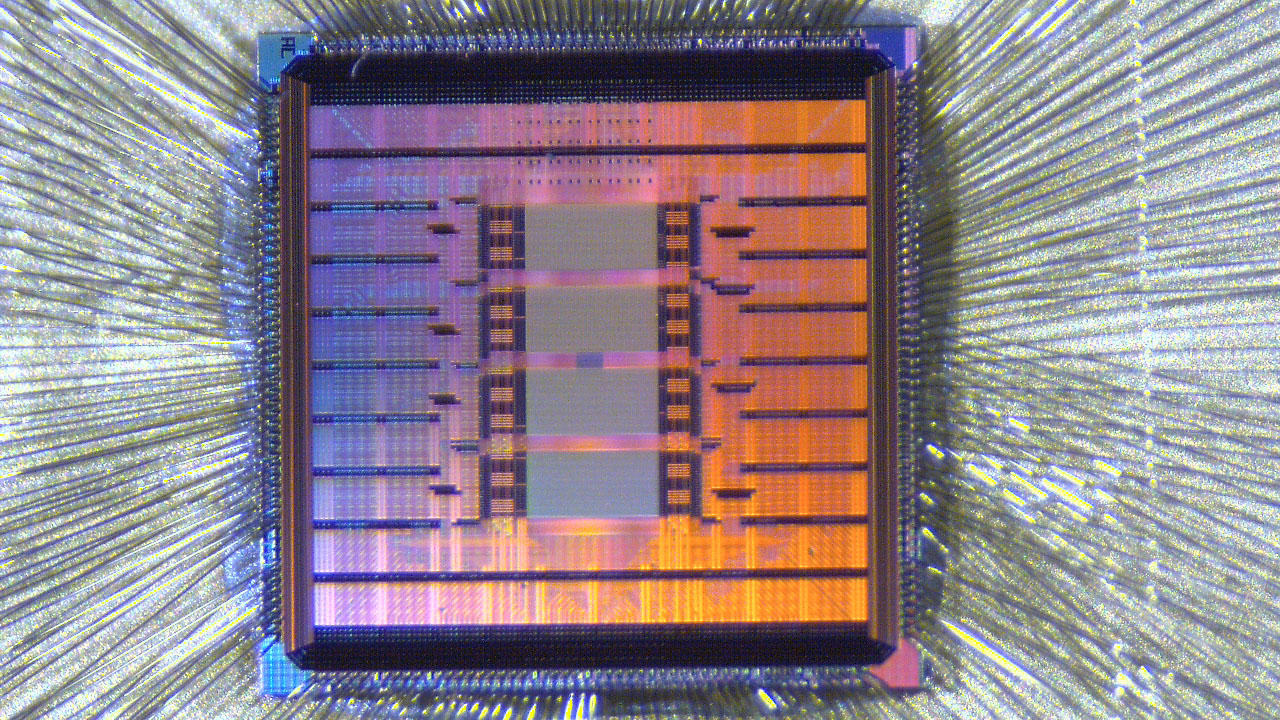
The Commerce Department said the silicon wafers will be base layer chips with specialized structures that will enable researchers to measure and test the performance of components placed on top of them. This could include new types of memory devices, bioelectronics, nanosensors and other advanced devices needed to power artificial intelligence and quantum computing.
“Google, NIST and Skywater will produce semiconductor wafers — not chips — that researchers and others can use to explore and develop nanotechnology tools and solutions in areas such as microprocessor design and production,” said Charles King of Pund-IT Inc. “It does resonate with the Biden plan, but it seems more about easing and increasing the belief of research projects, as opposed to short-term commercial silicon production. Discussions about the effort also began months before the Biden plan was announced.”
Holger Mueller of Constellation Research Inc. said the U.S. government is essentially trying to “prime the pump” for local chip production with today’s initiative, which was actually planned long before the CHIPS Act was dreamed up. “The partnership involves Google’s funding, NIST designing the chips and Skywater manufacturing them,” Mueller explained. “The main benefit is that research institutions will be able to build higher-level chips. It’s a long-term project, so it will be a few years before we can tell if the initiative will help the U.S. become a leader in chip manufacturing once again. It’s a promising start, though.”
NIST said the new chips will be made available to researchers as 200-millimeter discs of patterned silicon. Researchers will then be able to slice and dice these as required into thousands of individual chips. Modern computer chips are built using stacked components, with the semiconductor sitting at the bottom layer and more specialized components sitting on top.
Google Public Sector Chief Executive Will Grannis said his company has a long history of leadership in the open-source world. “Moving to an open-source framework fosters reproducibility, which helps researchers from public and private institutions iterate on each other’s work,” he said. “It also democratizes innovation in nanotechnology and semiconductor research.”
Support our mission to keep content open and free by engaging with theCUBE community. Join theCUBE’s Alumni Trust Network, where technology leaders connect, share intelligence and create opportunities.
Founded by tech visionaries John Furrier and Dave Vellante, SiliconANGLE Media has built a dynamic ecosystem of industry-leading digital media brands that reach 15+ million elite tech professionals. Our new proprietary theCUBE AI Video Cloud is breaking ground in audience interaction, leveraging theCUBEai.com neural network to help technology companies make data-driven decisions and stay at the forefront of industry conversations.