


 INFRA
INFRA
INFRA
INFRA
INFRA
Intel Corp. today announced that it has begun mass-producing chips using extreme ultraviolet lithography, or EUV, the most advanced semiconductor manufacturing technology on the market.
The company reached the milestone at its Fab 34 plant in Leixlip, Ireland. Intel has equipped the plant with EUV capabilities as part of a €17 billion investment plan it launched in 2019. In the coming years, it plans to spend many tens of billions more to bring additional EUV production lines online around the world.
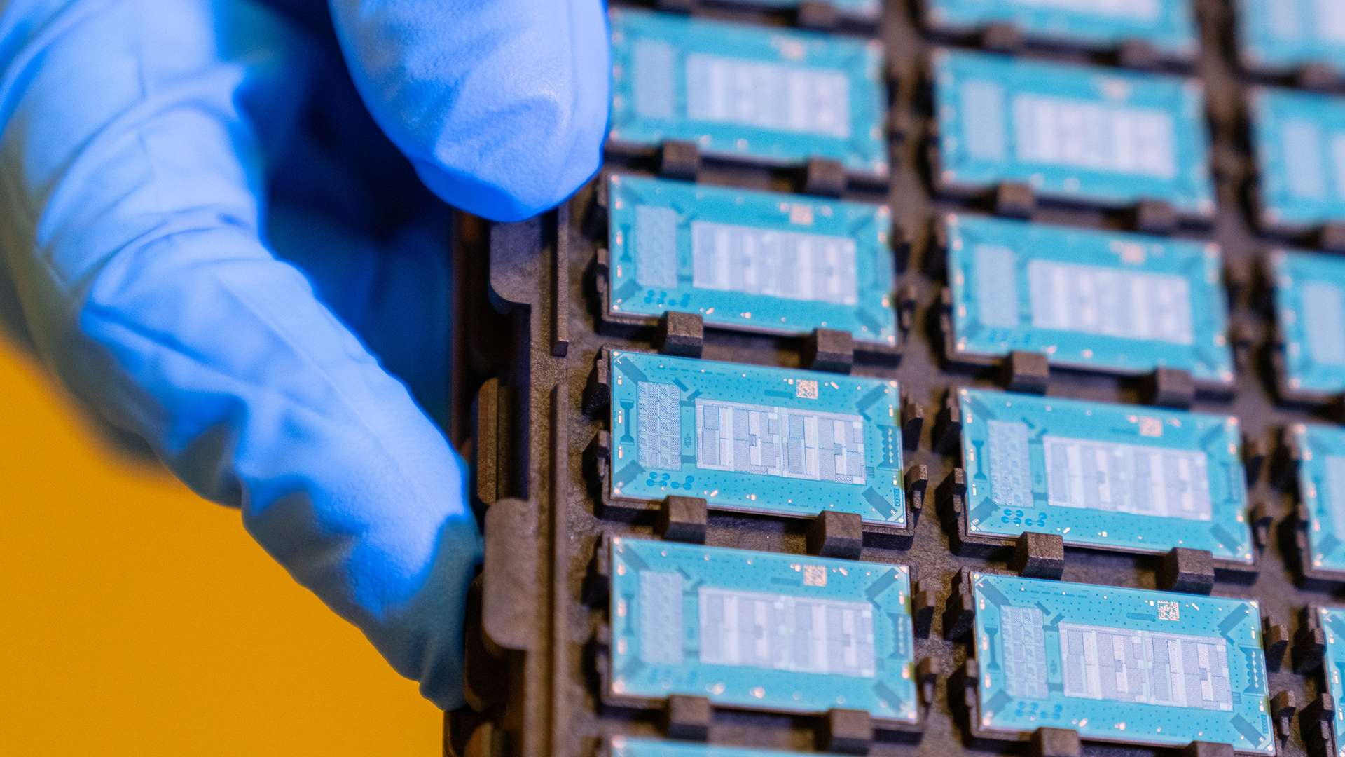
Intel’s Leixlip fab will initially use the new production equipment to make Meteor Lake laptop processors (pictured). The chips are based on the company’s Intel 4 process, which corresponds to rivals’ seven-nanometer nodes. Each Meteor Lake processor comprises five miniature chips, or chiplets. Four contain computing components and the fifth functions as the foundation on which the others sit.
“The Silicon Isle has always been core to our long-term strategy, and today’s opening of Fab 34 contributes to the EU’s goal of creating a more resilient and sustainable semiconductor supply chain,” said Intel Chief Executive Officer Pat Gelsinger.
EUV chipmaking equipment is made exclusively by ASML Holding NV, a Dutch company with a market capitalization about $50 billion higher than Intel. Each of its EUV machines costs $150 million and takes up as much space as a school bus. The company recently upped its revenue forecast amid record demand from chipmakers.
The reason EUV technology is needed stems from the fact that the size of transistors has shrunk dramatically over the past few decades. Transistors are carved from a piece of solid material much like a statue. The smaller the statue, the finer the tools necessary to create it.
ASML’s EUV machines carve transistors into silicon wafers using beams of ultraviolet light. An ultraviolet light beam has a significantly shorter wavelength than visible light. As a result, an EUV machine can carve smaller transistors into silicon than earlier lithography systems that rely on longer light beams.
Using ultraviolet light for chip manufacturing involves numerous technical challenges that took researchers decades to overcome. EUV machines address those challenges with a combination of lasers, mirrors and magnetically levitating wafer trays that accelerate faster than a plane. The complexity of those components is the reason the systems cost about $150 million apiece.
An EUV machine produces ultraviolet light by shining two laser beams on a tiny piece of lead. The first beam flattens the metal, while the second vaporizes it. This process is repeated about 50,000 times per second to produce a series of high-frequency ultraviolet light pulses.
Light travels from inside an EUV machine onto the silicon wafers being turned into chips by bouncing through a series of mirrors. Those mirrors are made from more than 100 layers of material. According to ASML, they are polished until their surface is even to within one atom’s thickness.
EUV machines require such delicate components because ultraviolet light is easily absorbed. In the past, chipmaking machines focused their light on wafers not by bouncing it around with mirrors but rather by beaming it through a transparent lens. Ultraviolet light can’t pass through a lens because it would be absorbed by the glass, which is why ASML opted for a mirror-based approach.
Silicon wafers enter an EUV machine by traveling on magnetically levitating trays. The EUV machine carves transistors into the wafers by shining beams of ultraviolet light onto their surface.
Intel’s top rivals, namely Taiwan Semiconductor Manufacturing Co. Ltd. and Samsung Electronics Co. Ltd., have long used EUV machines to make processors. The company is now spending tens of billions of dollars on its manufacturing infrastructure in a bid to catch up. Intel has set a goal of rolling out five new manufacturing processes in four years.
As part of its longer term plans, Intel last year signed a contract to buy the first of ASML’s upcoming High NA EUV machines. Those machines feature more advanced optical technology that the EUV equipment the company currently sells. According to ASML, they can carve transistors into wafers with a resolution up to 70% higher than current-generation hardware and process more wafers per hour.
High NA EUV machines will make it easier for Intel to continue improving its transistors. The company and its rivals are currently switching to a new type of transistor design, known as a gate-all-around architecture, that is more complicated to implement than today’s technology. The increased resolution and manufacturing speed of ASML’s High NA EUV machines should simplify the task of mass producing gate-all-around processors.
Support our mission to keep content open and free by engaging with theCUBE community. Join theCUBE’s Alumni Trust Network, where technology leaders connect, share intelligence and create opportunities.
Founded by tech visionaries John Furrier and Dave Vellante, SiliconANGLE Media has built a dynamic ecosystem of industry-leading digital media brands that reach 15+ million elite tech professionals. Our new proprietary theCUBE AI Video Cloud is breaking ground in audience interaction, leveraging theCUBEai.com neural network to help technology companies make data-driven decisions and stay at the forefront of industry conversations.