 INFRA
INFRA
 INFRA
INFRA
 INFRA
INFRA
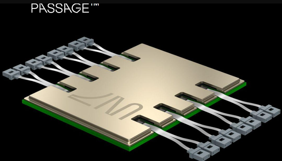
The silicon photonics pioneer Lightmatter Inc. says it’s ready to spearhead a revolution in data center connectivity with the coming launch of its first 3D co-packaged optics product, Passage L200.
The Passage L200, which will be available in 32 terabyte and 64TB flavors, is designed to integrate with the latest graphics processing units and networking switch designs to speed up chip-to-chip communications and eliminate the bottlenecks created by today’s existing chip interconnects. It can support massive clusters of thousands of GPUs with unprecedented bandwidth.
In addition to its first CPO, Lightmatter also unveiled the Passage M1000 reference platform for a 3D Photonic Superchip, designed for customers to create their own customized GPU interconnects that utilize silicon photonics. It’s a “multi-reticle active photonic interposer” that makes it possible for customers to create larger die complexes on silicon wafers to enhance connectivity for large-scale GPU clusters.
Lightmatter, which came to prominence last year after raising $400 million in a Series D funding, is one of the leading players in the nascent silicon photonics industry, seeking to transform how GPUs and other chips communicate and exchange data with each other. It’s aiming to provide much higher bandwidth and lower-latency connections using optical fiber connections, so enterprises can scale their data centers to support more powerful artificial intelligence applications and high-performance computing workloads.
In an interview with SiliconANGLE last year, Lightmatter Chief Executive Nick Harris explained that GPUs have increased their processing power in terms of operations per second by more than 1,000 times. Those gains, which took place in less than a decade, mean that even the fastest network interconnects, used to link clusters of GPUs, cannot even hope to keep up with the number of computations they can perform.
In the AI industry, it has become essential for companies to link thousands or even tens of thousands of GPUs together, so they can work in concert to power the most advanced large language models. However, with the improvements in GPU processing, the interconnects that support these clusters have become the weakest link. GPUs are constantly having to wait for data to arrive, which means they spend most of their time sitting idle instead of processing information.
“If you’re one of these GPUs, your life is like: OK, I’m waiting for data from memory, crunch, crunch, crunch, OK, waiting for data from another GPU, crunch, crunch, crunch, and just sitting there,” Harris told SiliconANGLE last year. “Only 30% of the time you’re doing calculations. So, you’ve got this Ferrari engine, it’s in Manhattan, and there’s stoplights everywhere.”
As a result, the main bottleneck for AI these days is the ability of GPUs to communicate with one another. Solve this and it should be possible to accelerate AI to unprecedented speeds, and that’s the promise Lightmatter is making with its new Passage L200 and Passage M1000 3D co-packaged optics.
Lightmatter’s Passage solves the problem of cumbersome networking interconnects by interposing its ultra-dense optical fiber technology with data center chips to improve bandwidth by as much as 100 times compared to the best solutions in use today. Essentially, it combines its fiber optic interconnects directly into a package of silicon chips.
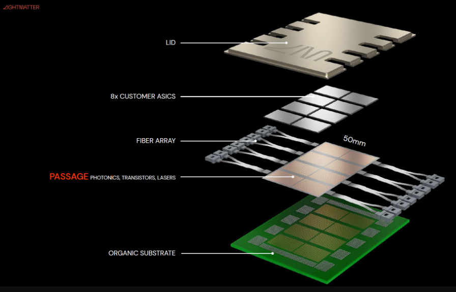
The Passage L200 CPO chips, which are expected to launch next year, and the Passage M1000 reference design, which will be made available this summer, are said to shatter existing interconnect bottlenecks. The most powerful 64TB L200 enables multiple GPUs to be packaged together on a single chip to provide more than 200 terabytes per second of input/output bandwidth, speeding up AI training and inference by more than eight times, the company says.
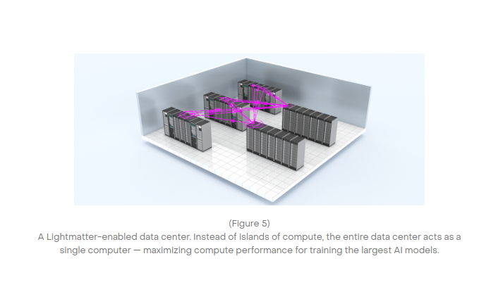
In traditional data centers, GPUs are interconnected using an array of networked switches that form a kind of layered hierarchy. But this architecture creates too much latency, because for one GPU to talk to another, it must go through multiple switches to reach it.
Harris said Lightmatter flattens that hierarchy. “So instead of six or seven layers of switches, you’ve got two, and each GPU can connect to thousands of others,” he explained.
Lightmatter refers to its novel interconnect architecture as “edgeless I/O,” and says it can scale bandwidth across the entire die area on any GPU. In the context of integrated circuits, a die refers to the individual circuits integrated onto silicon wafers. GPUs contain thousands of these dies, all working in unison to crunch and process data. Traditional dies can only connect to other dies at the “shoreline,” essentially at the edge of each die. Lightmatter, on the other hand, allows I/O connectivity anywhere on the surface of the die, vastly increasing the bandwidth it supports.
The company said the upcoming L200 CPO is engineered for high-volume manufacturing, and it’s working closely with semiconductor fabrication partners like Global Foundries Inc. to facilitate production-readiness.
“The Shoreline is no longer a limitation for I/O,” Harris said in a statement. “This is all made possible by our close co-engineering with leading foundry and assembly partners and our supply chain ecosystem.”
Support our mission to keep content open and free by engaging with theCUBE community. Join theCUBE’s Alumni Trust Network, where technology leaders connect, share intelligence and create opportunities.
Founded by tech visionaries John Furrier and Dave Vellante, SiliconANGLE Media has built a dynamic ecosystem of industry-leading digital media brands that reach 15+ million elite tech professionals. Our new proprietary theCUBE AI Video Cloud is breaking ground in audience interaction, leveraging theCUBEai.com neural network to help technology companies make data-driven decisions and stay at the forefront of industry conversations.