


 EMERGING TECH
EMERGING TECH
EMERGING TECH
EMERGING TECH
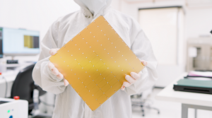
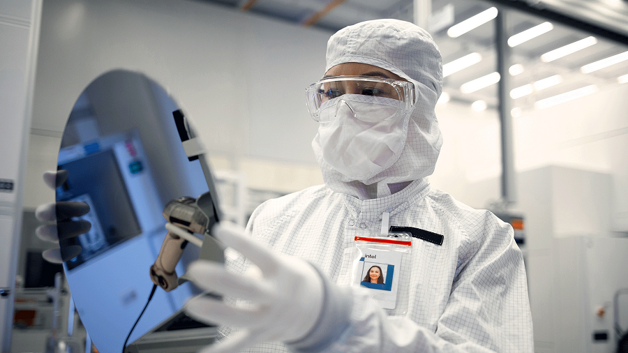
Intel Corp. has shared new information about Intel 14A, an upcoming chip manufacturing process that will use ASML Holding NV’s most advanced lithography machines.
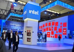
Executives detailed the process today at an event dedicated to the company’s foundry business. The business makes processors for other organizations using Intel fabs. Alongside Intel 14A, the chipmaker detailed other upcoming manufacturing processes and three new packaging technologies.
“Intel is committed to building a world-class foundry that serves the growing need for leading-edge process technology, advanced packaging and manufacturing,” said Intel Chief Executive Officer Lip-Bu Tan.
According to Tom’s Hardware, Intel 14A will be powered by ASML’s High NA EUV lithography machines. The most advanced lithography equipment used in production today etches transistors into silicon wafers with a resolution of 13.5 nanometers. ASML’s High NA EUV machines have an eight-nanometer resolution, which allows them to form smaller transistors. Each system is the size of a double-decker bus and costs about $350 million.
In current processors, transistors sit below a stack of tiny wires that supplies them with electricity and data. Chipmakers are starting to move the wires that carry electricity below the transistors, which improves power efficiency. This arrangement is known as backside power delivery.
Intel’s first implementation of backside power delivery is expected to start shipping with its chips this year. The upcoming Intel 14A node will reportedly use a second-generation implementation called PowerDirect. The technology boosts energy-efficiency by connecting power delivery wires to each transistor’s source and drain, the components through which electrons enter and leave the circuit, respectively.
It’s unclear when Intel 14A will enter mass production. However, the chipmaker did detail that several customers have already expressed interest in using the technology. Intel has provided those customers with development kits that they can use to familiarize themselves with the upcoming process.
At today’s foundry event, the company also shared an update about another upcoming process called Intel 18A. It’s less advanced than Intel 14A and will roll out earlier. Executives disclosed that the process is already being used to make chips in limited volumes and will begin mass production later this year.
Intel 18A will be available in multiple editions. One version, Intel 18A-P, provides increased performance that makes it suitable for making data center chips. Another edition called Intel 18A-PT will enable customers to produce processors in which multiple chiplets are stacked atop one another.
Intel will roll out the upcoming manufacturing processes alongside new packaging options. Packaging is the technology that makes it possible to link multiple chiplets into a single processor.
One of the new technologies, EMIB-T, will connect chiplets to one another using tiny wires called through-silicon vias. It will be joined by two other new packaging systems called Foveros-R and Foveros-B. The latter offering is geared toward cost-sensitive chips such as those that are used in consumer devices, while the latter is optimized for data center environments.
Support our mission to keep content open and free by engaging with theCUBE community. Join theCUBE’s Alumni Trust Network, where technology leaders connect, share intelligence and create opportunities.
Founded by tech visionaries John Furrier and Dave Vellante, SiliconANGLE Media has built a dynamic ecosystem of industry-leading digital media brands that reach 15+ million elite tech professionals. Our new proprietary theCUBE AI Video Cloud is breaking ground in audience interaction, leveraging theCUBEai.com neural network to help technology companies make data-driven decisions and stay at the forefront of industry conversations.