


 INFRA
INFRA
INFRA
INFRA
INFRA
ChEmpower Corp., a semiconductor materials company that develops polishing pads and chemical solutions, today announced Chakra, its first product designed to improve efficiency, reduce costs and promote sustainability in the chipmaking process.
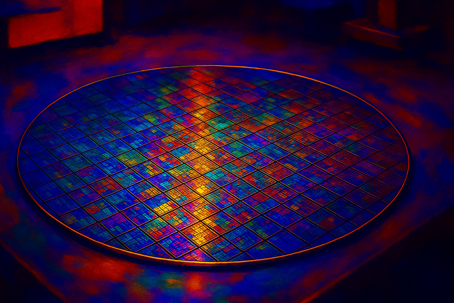
As semiconductors are etched and built up layer by layer, wafers must be planarized, or smoothed. This step, known as chemical mechanical planarization, requires grinding and polishing to remove excess material so that additional layers of circuitry can be laid down.
Conventional CMP uses a chemical solution and an abrasive slurry to grind away unwanted materials and create an ultra-smooth surface. But as modern integrated circuits stack more layers and tighter features, slurry particles can contribute to scratches, residue and other imperfections, which can lead to failures when the next layer is deposited.
ChEmpower eschews abrasive slurry in favor of functional polishing pads and a cleaner chemical process, with the goal of reducing surface damage, producing a more uniform finish and cutting wastewater.
“If you were to look at defect density targets… yield is a big issue,” Chief Executive Sudhanshu Misra, Ph.D., told SiliconANGLE in an interview. “The functional pad, in conjunction with the polish fluid, so that it offsets the use of abrasives, is what our abrasive-free transition technology is about.”
Misra’s headline claim is that Chakra’s pad actively participates in the chemistry, so planarization becomes chemically driven rather than primarily mechanical, especially in copper interconnect steps that are increasingly critical for advanced logic, high-bandwidth memory and advanced packaging.
Interconnects are microscopic metal wiring that link billions of transistors together on semiconductor surfaces, like metal roadways that allow signals and power move around the chip.
In advanced packaging, instead of placing chips side-by-side, they are stacked vertically, thus perfectly smooth planarization becomes essential and flat surfaces so they can be “glued” or bonded together without gaps. The most advanced methods chips are bonded copper-to-copper directly without any solder between and that is only possible if surfaces are polished to nanoscale flatness.
This shift in efficacy and technology, Misra argues, also has sustainability upside. The product’s chemistry avoids hazardous materials such as BTA, benzotriazole, a compound often discussed as problematic in industrial handling and disposal. It also produces an effluent stream that is easier to recover and recycle, including wastewater and dissolved copper salts, potentially reducing the overall water burden associated with CMP.
ChEmpower raised $18.7 million in April to commercialize Chakra and move the “minimum viable product” into pilots with multiple partners.
“We leveraged the funding to commercialize what we had as an MVP [and to] productize sufficiently so that it’s validated on commercial tools in a commercial fab-like environment,” Misra said.
He added that the company is already working with a handful of “top-notch” memory and logic companies in the United States and Asia, with pilots and trials that are expanding.
Misra described Chakra as the first commercial product in a multi-material roadmap. ChEmpower is starting with copper interconnects, then intends to extend the technology to adjacent CMP steps, including barrier materials and oxide, with silicon polishing also on the horizon. The through line, he said, is using functional pads and chemistry to improve selectivity and surface quality as device stacks and packaging demands continue to tighten.
Support our mission to keep content open and free by engaging with theCUBE community. Join theCUBE’s Alumni Trust Network, where technology leaders connect, share intelligence and create opportunities.
Founded by tech visionaries John Furrier and Dave Vellante, SiliconANGLE Media has built a dynamic ecosystem of industry-leading digital media brands that reach 15+ million elite tech professionals. Our new proprietary theCUBE AI Video Cloud is breaking ground in audience interaction, leveraging theCUBEai.com neural network to help technology companies make data-driven decisions and stay at the forefront of industry conversations.