 INFRA
INFRA
INFRA
INFRA


INFRA

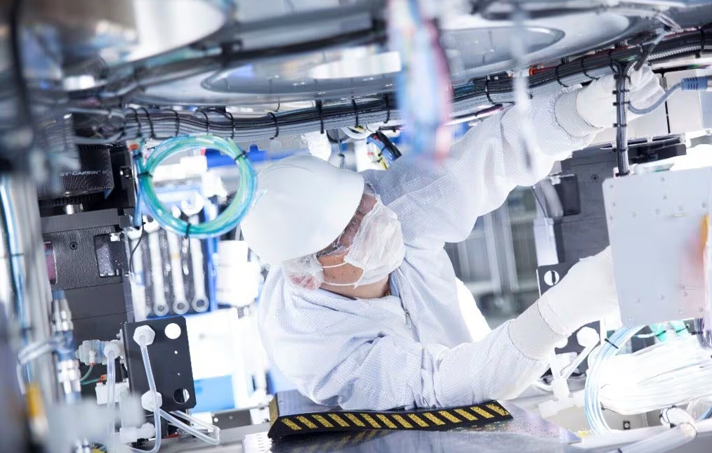
Chipmaking equipment giant Applied Materials Inc. is trying to make life easier for its chip fabrication plant customers, so they can build the extremely complex 3D architectures necessary for the next generation of artificial intelligence processors.
To do this, it has unveiled a host of new chip fabrication systems that span advanced packaging, process control and dynamic-random access memory manufacturing. The new machinery will help semiconductor manufacturers to increase their production volumes and yields for more sophisticated, powerful and energy efficient chips, which stretch their existing manufacturing capabilities to the limit.
Applied Materials is trying to help chip companies overcome what’s known in AI infrastructure circles as the “memory wall.” As AI models become more powerful and capable, existing silicon processors can no longer keep pace with their extreme memory and bandwidth demands. To overcome this challenge, most chipmakers have gravitated toward more advanced packaging architectures that involve 3D stacking techniques and the use of high-bandwidth memory components.
But 3D stacking is extremely complex. The process requires multiple DRAM chips to be stacked on top of one another and connected using microscopic through-silicon vias or TSVs. It can dramatically increase the data throughput of processors, but manufacturing these chips is an extremely intricate process. Add in the problem of shrinking dimensions, uneven interconnects and the physical fragility of these ultra-thin processors, and it becomes almost impossible to manufacture them without high defect rates that eat away at production yields.
Applied Materials says its new systems are designed to overcome these problems, targeting the most intricate aspects of advanced packaging. The new products include three novel systems for chemical mechanical polarization and deposition.
Applied’s Opta Quad CMP platform has been built to smooth out thicker films and hybrid bonds with unprecedented precision. The system continuously monitors the silicon wafers throughout the manufacturing process, dynamically adjusting them in real time to ensure perfect surface planarity.
The company also introduced the Nokota Vmax 2 ECD system, which is designed to solve the challenge of uneven interconnects. It relies on adaptive pattern tuning to create high-precision copper plating that ensures the TSVs and microbumps can be leveled out perfectly across the wafer and prevent gaps between the 3D layers.
Meanwhile, Producer Avila 2 PECVD is designed to address issues around the physical warping of ultra-thin chips. Modern high-bandwidth memory dies are about 25 times thinner than standard silicon wafers, which makes them extremely susceptible to deformation. Applied says the new system can fix this by depositing stress-balanced dielectric films around the vias to enhance their stability, enabling chipmakers to stack 12, 16 or potentially even more layers without any bonding issues.
With regard to process control, Applied Materials has announced a pair of new electron-beam systems, including the VeritySEM 7AP and the SEMVision G7AP, which aim to catch the microscopic defects that can ruin 3D-stacked HBM packages. The tools feature sub-10-nanometer sensitivity, enabling them to measure and review defects on heterogeneous substrates, so chipmakers can catch critical flaws and stray particles that are too small to be spotted by existing optical inspection tools.
Last but not least, Applied Materials says its new Enhanced Centura Prime Epi system can help to improve the performance of the actual memory chips. It brings advanced, logic-class epitaxy to the DRAM manufacturing process in order to increase transistor efficiency, the company explained. It claims to enable more power-efficient memory operations, with the machine itself having a 20% smaller factory footprint.
Support our mission to keep content open and free by engaging with theCUBE community. Join theCUBE’s Alumni Trust Network, where technology leaders connect, share intelligence and create opportunities.
Founded by tech visionaries John Furrier and Dave Vellante, SiliconANGLE Media has built a dynamic ecosystem of industry-leading digital media brands that reach 15+ million elite tech professionals. Our new proprietary theCUBE AI Video Cloud is breaking ground in audience interaction, leveraging theCUBEai.com neural network to help technology companies make data-driven decisions and stay at the forefront of industry conversations.