


 NEWS
NEWS
NEWS
NEWS
NEWS
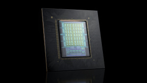
 Electrical engineers have already achieved some pretty amazing feats. The integrated circuits used in everything from computers to coffee makers are incredibly slim these days, allowing us to develop a new breed of electronic gadgets that includes everything from every day smartphones, to more minuscule devices like the Picotux (the world’s smallest PC, measuring just 35mm×19mm×19mm) and even fuel cells measuring just 3mm long.
But these achievements haven’t stopped researchers from Cornell University from thinking they can take ‘slim’ to a whole new level – an atomic level to be precise.
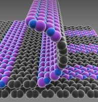
Using substances called graphene (a semi-conductor) and hexagonal boron nitride (an insulator), which are basically one atom-thick sheets of repeating atoms, researchers led by Jiwoong Park have opened a new frontier in nano-scale electronics.
Their technique, which they’ve termed patterned regrowth, involves the precise placement of atoms on these sheets in order to manipulate their electronic properties, and could possibly lead to the development of next-generation electronic circuits – transparent circuit boards that are so thin they could easily float on the surface of water, or even on air, while maintaining both their rigidity and a high level of efficiency.
Graphene and boron nitride are grown using a process known as photolithography, which ensures that the sheets are perfectly smooth and flat, with no creases or bumps, making them ideal substances for an atomically thin circuit.
Park likened the technique for making his circuits to that of stenciling; firstly, the graphene was grown on a copper base; next, selected areas of the copper underneath the graphene were exposed, in order to create a ‘pattern’ for their circuit. These exposed areas were then filled in with boron nitride, which also grows well on copper and fills all of these ‘gaps’ perfectly.
The end result is a microscopically thin ‘film’ that can easily be peeled off its copper base and used as an electronic circuit, with the graphene atoms acting as the ‘wire’ and the boron nitride assuming the role of the circuit board.
Cool stuff to be sure, but the best thing about it is that researchers believe that the process for making atomic circuit boards may soon commercially viable. The researchers are already highly-skilled in growing graphene, and the photolithography technique is widely used in the production of integrated circuits on flat silicone. With a little refinement, a future of genuinely transparent electronics might not be that far off.
Support our mission to keep content open and free by engaging with theCUBE community. Join theCUBE’s Alumni Trust Network, where technology leaders connect, share intelligence and create opportunities.
Founded by tech visionaries John Furrier and Dave Vellante, SiliconANGLE Media has built a dynamic ecosystem of industry-leading digital media brands that reach 15+ million elite tech professionals. Our new proprietary theCUBE AI Video Cloud is breaking ground in audience interaction, leveraging theCUBEai.com neural network to help technology companies make data-driven decisions and stay at the forefront of industry conversations.