


 INFRA
INFRA
INFRA
INFRA
INFRA
Japan’s Kyocera Corp. will invest 1.3 trillion yen, or $9.78 billion, through March 2026 to build new chip component plants and expand its capabilities in other areas.
Nikkei Asia reported the plan today. The $9.78 billion that Kyocera intends to spend over the next three years includes capital expenditures such as plant construction, as well as research and development costs. According to today’s report, the planned investment approximately doubles what Kyocera spent on the same items during the previous three years.
Kyoto-based Kyocera makes a wide range of products ranging from printers to solar panels. It’s also a major manufacturer of chip components. The company supplies components for vehicle processors, data center networking devices and a range of other systems.
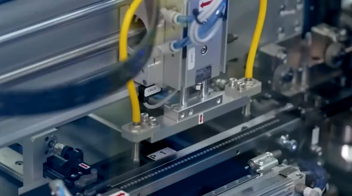
Chips such as central processing units are usually deployed in a specialized case known as a semiconductor package. The semiconductor package shields the chip that it contains from potential sources of damage. It also helps dissipate heat, while providing wires for connecting to other electronic components.
As part of its planned $9.8 billion investment, Kyocera will build a new semiconductor package plant in Japan’s Kagoshima prefecture. Construction of the plant is expected to cost about 60 billion yen, or $450 million.
The company will also build a new manufacturing facility in Nagasaki that will reportedly focus on making “ceramic components and semiconductor packaging.” Many semiconductor packages are made of ceramic materials. The facility will reportedly cost up to 100 billion yen, or $749 billion, to build and is expected to begin production in 2026.
According to Nikkei Asia, Kyocera also plans to expand a number of existing plants that make multifunctional printers and quartz components. It’s a major producer of crystal oscillators, a type of circuit that is often made from quartz and helps regulate processors’ clock speed.
Kyocera reportedly plans to fund its planned investment by borrowing up to 1 trillion yen. The company is expected to use its 15% stake in KDDI Corp., Japan’s second largest telecommunications company, as collateral for the debt financing. It will reportedly begin borrowing before March 2023 with the goal of raising up to 500 billion yen over the following three years.
Intel Corp. is also expected to increase its investment in chip package technologies over the next few years. In August, sources told Reuters that the company plans to spend up at least $5 billion on a new chip packaging and assembly facility in Italy. It has reportedly picked Vigasio, a town located about 68 miles west of Venice, as the preferred site of the facility.
Several of Intel’s upcoming processors are set to include a new semiconductor package technology called Foveros. The technology makes it possible to stack multiple chip modules, or chiplets, atop one another in a three-dimensional configuration. One of the first Intel products to feature Foveros will be its Xeon GPU Max artificial intelligence processor, which features 47 chiplets with 100 billion transistors.
Support our mission to keep content open and free by engaging with theCUBE community. Join theCUBE’s Alumni Trust Network, where technology leaders connect, share intelligence and create opportunities.
Founded by tech visionaries John Furrier and Dave Vellante, SiliconANGLE Media has built a dynamic ecosystem of industry-leading digital media brands that reach 15+ million elite tech professionals. Our new proprietary theCUBE AI Video Cloud is breaking ground in audience interaction, leveraging theCUBEai.com neural network to help technology companies make data-driven decisions and stay at the forefront of industry conversations.