


 INFRA
INFRA
INFRA
INFRA
INFRA
Intel Corp. is poised to receive as much as $19.5 billion in federal funding and loans to expand its domestic chipmaking infrastructure.
The Commerce Department will provide the financing through a preliminary, nonbinding memorandum of terms that officials announced today. Under the agreement, Intel will receive up to $8.5 billion in direct funding and the option to draw upon as much as $11 billion worth of loans. The deal is expected to be the largest grant issued under the 2022 CHIPS and Science Act.
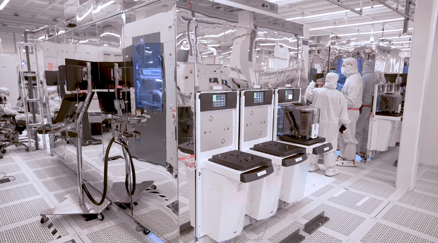
The federal financing will support Intel’s plans to spend more than $100 billion over five years to expand its domestic fab network. The company is building chip plants and research centers across sites in Arizona, New Mexico, Ohio and Oregon. Intel will be eligible to receive a Treasury Department tax credit of up to 25% on the planned investment.
“Today is a defining moment for the U.S. and Intel as we work to power the next great chapter of American semiconductor innovation,” said Intel Chief Executive Officer Pat Gelsinger. “CHIPS Act support will help to ensure that Intel and the U.S. stay at the forefront of the AI era as we build a resilient and sustainable semiconductor supply chain to power our nation’s future.”
According to the Financial Times, most of the funds will go toward developing the company’s Intel 18A process. The technology is the center of the chipmaker’s efforts to catch up with Taiwan Semiconductor Manufacturing Co. in transistor quality. Executives have projected that Intel 18A will enable the chipmaker to “regain process leadership” when it comes online in 2025.
Intel 18A is expected to form the basis of an upcoming server system-on-chip family called Clearwater Forest. According to IEEE Spectrum, the processors in the series can theoretically be equipped with up to 300 billion transistors. Nvidia Corp.’s new Blackwell B200 flagship graphics card features about 208 billion transistors.
Each Clearwater Forest processor will feature three sets of chiplets stacked atop one another in a three-dimensional configuration. One set of chiplets will contain logic circuits, or transistors designed for carrying out computations. The remaining chiplets will include the processor’s cache, voltage regulators and other auxiliary components.
Intel is expected to start shipping processors with a new gate-all-around, or GAA, transistor architecture in the second half of 2024. The logic circuit chiplets in Clearwater Forest are set to use an improved, second-generation version of that GAA architecture.
An Intel processor is made of numerous modules, or cells, that each contain a relatively small number of transistors. The Intel 18A process will make it possible to include GAA transistors with different physical dimensions in the same cell. According to Intel, that customizability will enable its engineers to develop faster and more efficient circuits.
In Clearwater Forest processors, only the chiplets that include logic circuits are made using Intel 18A. The chiplets containing auxiliary components such as voltage regulators will be produced using earlier manufacturing processes. The reason is that those auxiliary components improve at a slower pace over time than Moore’s Law, which means they can’t take full advantage of the performance benefits offered by Intel 18A.
One focus of Intel’s $100 billion infrastructure investment plan is its New Mexico chipmaking hub. At the start of the year, the company expanded the campus with a new facility called Fab 9. The facility will make 3D packaging components, the hardware Intel uses to link together the chiplets in vertically-stacked processors such as Clearwater Forest.
The chiplets in each Clearwater Forest processor are linked together using a new packaging technology called Foveros Direct 3D. According to Intel, it provides the ability to place 16 times more connections between chiplets than its current-generation hardware. That will translate faster data transfer speeds, which should improve processing speeds.
Foveros Direct 3D uses a layer of copper placed on the surface of a processor’s chiplets to move data between them. After two chiplets are stacked atop one another during manufacturing, the copper layers are heated, which causes them to bind together. This creates a hardware link that allows electric signals to rapidly move between a processor’s different modules.
“With this agreement, we are helping to incentivize over $100 billion in investments from Intel – marking one of the largest investments ever in U.S. semiconductor manufacturing, which will create over 30,000 good-paying jobs and ignite the next generation of innovation,” said U.S. Secretary of Commerce Gina Raimondo.
Intel’s infrastructure investments will create 10,000 jobs at the company along with 20,000 construction positions. Additionally, the chipmaker expects to indirectly support more than 50,000 jobs across its suppliers and other organizations. The funds allocated to the initiative under the CHIPS and Science Act are set to start arriving later this year.
Support our mission to keep content open and free by engaging with theCUBE community. Join theCUBE’s Alumni Trust Network, where technology leaders connect, share intelligence and create opportunities.
Founded by tech visionaries John Furrier and Dave Vellante, SiliconANGLE Media has built a dynamic ecosystem of industry-leading digital media brands that reach 15+ million elite tech professionals. Our new proprietary theCUBE AI Video Cloud is breaking ground in audience interaction, leveraging theCUBEai.com neural network to help technology companies make data-driven decisions and stay at the forefront of industry conversations.