


 INFRA
INFRA
INFRA
INFRA
INFRA
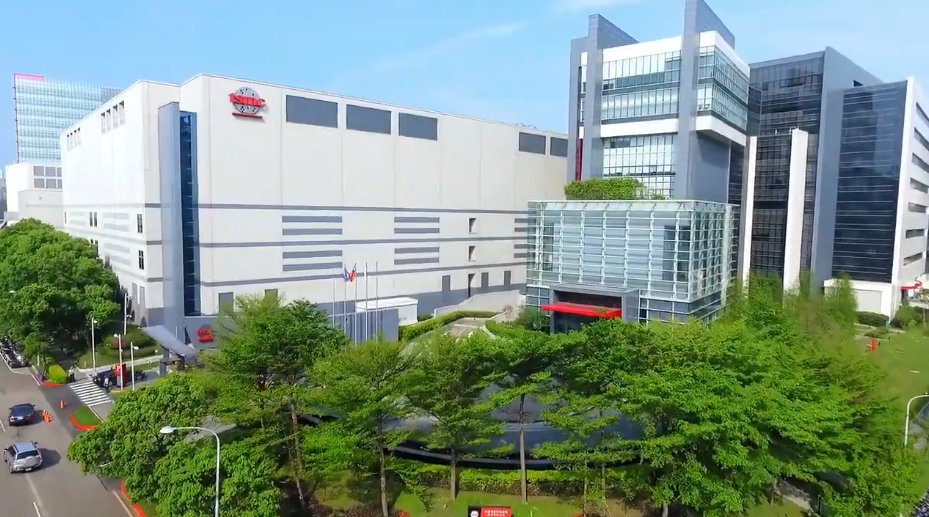
Taiwan Semiconductor Manufacturing Co. Ltd. has won $11.6 billion worth of federal financing to build a third chip fab in Phoenix, Arizona, the White House announced today.
The funds will be provided through a preliminary agreement the company has inked with the U.S. Commerce Department. The first tranche of funding is expected to arrive in a few months, once the agreement is finalized. TSMC will receive the rest in phases subject to the fulfillment of construction and chip production volume milestones.
Grants account for more than half of the financing the company is set to receive, or $6.6 billion, while the remaining $5 billion is set to arrive in the form of loans. The financing agreement stipulates that TSMC must spend $50 million on workforce development initiatives to train local workers. The project will create 6,000 manufacturing jobs and more than 20,000 construction positions.
“TSMC’s renewed commitment to the United States, and its investment in Arizona represent a broader story for semiconductor manufacturing that’s made in America and with the strong support of America’s leading technology firms to build the products we rely on every day,” President Joe Biden said in a statement.
The fab, which is expected to cost $25 billion, will operate alongside two other chip plants TSMC is currently building in Phoenix. The combined cost of the facilities is expected to exceed $65 billion. Two of the fabs, including the one for which TSMC secured federal financing today, will be capable of making two-nanometer chips.
TSMC’s two-nanometer node, the next major evolution of its chip production technology, is expected to enter mass production next year. It’s set to introduce two major innovations: a gate-all-around, or GAA, transistor design and backside power delivery.
The main feature of the GAA design is that the gate, the component which controls the flow of electricity within a transistor, surrounds the transistor’s other core components from all sides. This makes it more difficult for power to leak from the transistor, a major issue in chip design. Reducing the amount of electricity that a processor’s circuits waste makes it more power-efficient.
The other major feature of TSMC’s two-nanometer node also relates to power management. In a traditional chip, the transistors receive electricity through tiny wires located immediately above them. TSMC’s two-nanometer processors, in contrast, will place the power delivery wires below the transistors rather than above them.
Moving the wires beneath the transistors leaves more space above them for other components. As a result, those components can be placed farther apart. Increasing the distance between a circuit’s components allows engineers to decrease the interference between their respective electric fields, which increases processor efficiency.
Backside power delivery also has certain other benefits. Intel Corp.’s implementation of the technology, for example, allows transistors to be placed closer together. The reduced distance means data takes less time to travel between transistor clusters, which speeds up data processing.
TSMC plans to roll out backside power delivery with the second version of its two-nanometer node. The upgraded process iteration is expected to come online in 2026, or about a year after the first version. In the longer term, TSMC also plans to introduce an edition of its two-nanometer node optimized specifically for producing high-performance chips such as server-grade artificial intelligence accelerators.
The company estimates that its first two Phoenix fabs will come online in 2025 and 2028, respectively. The plant for which TSMC secured financing today will become operational at an unspecified date before the end of the decade.
TSMC is the latest in a string of semiconductor suppliers to have received funding under the 2022 CHIPS and Science Act. Late last month, rival Intel won up to $19.5 billion worth of grants and loans to expand its U.S. fab network. Samsung Electronics Co. Ltd., meanwhile, is expected to receive more than $6 billion worth of CHIPS Act funding in the coming weeks.
Support our mission to keep content open and free by engaging with theCUBE community. Join theCUBE’s Alumni Trust Network, where technology leaders connect, share intelligence and create opportunities.
Founded by tech visionaries John Furrier and Dave Vellante, SiliconANGLE Media has built a dynamic ecosystem of industry-leading digital media brands that reach 15+ million elite tech professionals. Our new proprietary theCUBE AI Video Cloud is breaking ground in audience interaction, leveraging theCUBEai.com neural network to help technology companies make data-driven decisions and stay at the forefront of industry conversations.