


 INFRA
INFRA
INFRA
INFRA
INFRA
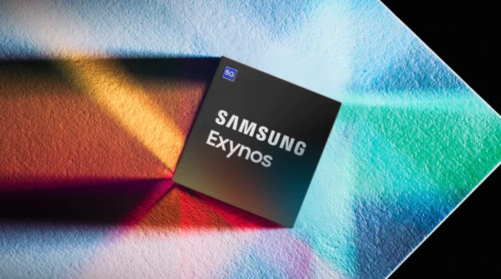
Samsung Electronics Co. Ltd. has previewed an upcoming chip manufacturing node, SF2, that will allow it to produce processors based on two-nanometer technology.
Executives detailed the node on Wednesday afternoon at an event hosted by the company’s semiconductor business. Alongside SF2, Samsung revealed several other upcoming chip manufacturing processes that it plans to bring online in the coming years.
SF2 is a new iteration of a node dubbed SF3P that the company first detailed last year. According to AnandTech, Samsung rebranded the technology to reflect the fact that its engineers have made several design improvements since the original announcement. The company is promising “notable power, performance and area benefits” for chips made with the upgraded SF2 node.
The first iteration of the process is set to come online. It will produce transistors based on a gate-all-around, or GAA, design. In the GAA architecture, the component tasked with coordinating the flow of electricity through a transistor surrounds the transistor’s core structure around all sides.
The technology has several advantage over earlier circuit designs. It reduces the amount of electricity that leaks from transistors during processing, which increases power efficiency. Additionally, the GAA architecture provides increased customizability, which allows engineers to more closely align processor designs with a project’s power efficiency and performance requirements.
The first iteration of Samsung’s SF2 node is scheduled to come online next year. It will be followed by an enhanced version, SF2P, that is set to launch in 2026 and will reportedly feature faster transistors. A third, even more advanced iteration slated to arrive in 2027 will add a feature called backside power delivery.
A modern processor’s transistors sit beneath a network of tiny wires made using the same lithography techniques. Some of those wires transmit data between the transistors, while others supply them with electricity. Samsung’s backside power delivery technology places the wires that carry electricity beneath the transistors rather than above them, which provides several benefits.
The technology helps improve chip performance by reducing so-called voltage droop. This is a phenomenon that causes sudden changes in the voltage of the electricity delivered to transistors. If they’re left unaddressed, those voltage changes can decrease processing speed and power efficiency.
Moving power delivery wires beneath a chip’s transistors also leaves more space for the data transmission wires that are located above those transistors. As a result, the data transmission wires can be placed further apart. This makes them easier to produce, which lowers manufacturing costs, and mitigates a type of technical issue called parasitic capacitance that can decrease chip performance.
The SF2 series of two-nanometer manufacturing processes is not the only new technology that Samsung detailed at its chip event. The company revealed that a new, enhanced version of its existing three-nanometer node will come online later this year. In parallel, Samsung is developing an enhanced version of its four-nanometer node that is set to launch in 2025.
The company also disclosed that work on its upcoming 1.4-nanometer process, the successor to SF2, is “progressing smoothly, with performance and yield targets on track for mass production in 2027.” In chip manufacturing, yield is a metric that measures production line reliability. The higher the yield, the fewer processors have to be discarded because of manufacturing faults, which in turn improves fab operators’ profitability and production volumes.
Support our mission to keep content open and free by engaging with theCUBE community. Join theCUBE’s Alumni Trust Network, where technology leaders connect, share intelligence and create opportunities.
Founded by tech visionaries John Furrier and Dave Vellante, SiliconANGLE Media has built a dynamic ecosystem of industry-leading digital media brands that reach 15+ million elite tech professionals. Our new proprietary theCUBE AI Video Cloud is breaking ground in audience interaction, leveraging theCUBEai.com neural network to help technology companies make data-driven decisions and stay at the forefront of industry conversations.