


 INFRA
INFRA
INFRA
INFRA
INFRA
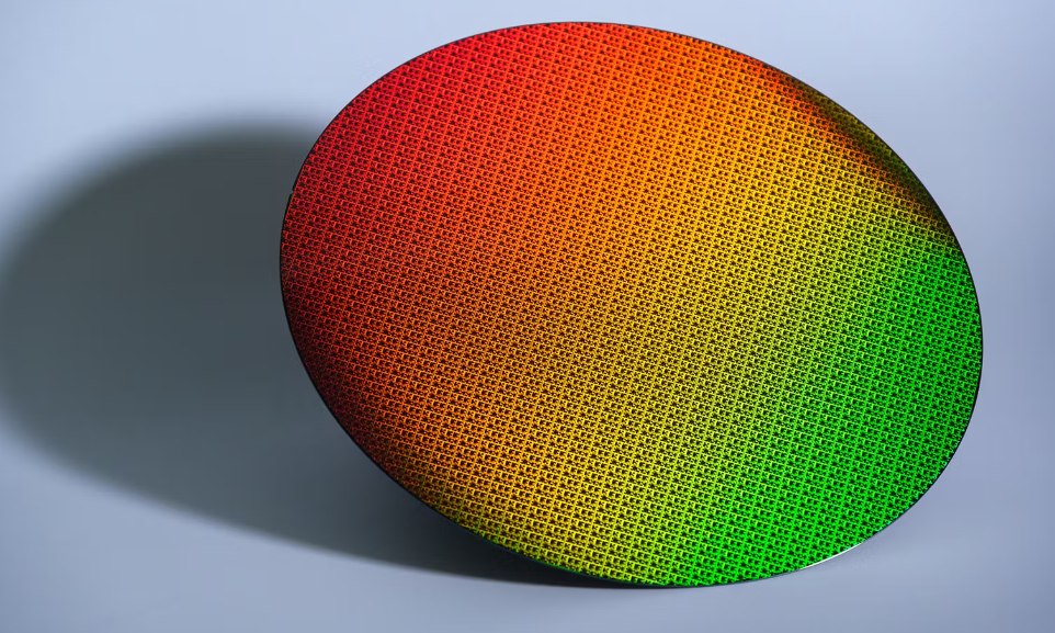
Intel Corp. finally had some good news to share for a change, providing an encouraging update on the progress of its most advanced 18A fabrication process, which will be used to manufacture a new generation of computer chips.
In today’s update, Intel said it has “powered on” two key products that will be the first to use the new production node, which involves a 1.8-nanometer-class process, referring to the size of the individual transistors. In addition, it announced the availability of a process design kit, which is essential for Intel Foundry customers that want to use the 18A process to create their own, customized chips.
Intel Foundry Services Senior Vice President and General Manager Kevin O’Buckley said the two products include Panther Lake, the latest generation of Intel’s mobile processors that will succeed the Lunar Lake and Arrow Lake chips that debuted earlier this year. The other is Clearwater Forest, a central processing unit for data center servers that’s destined to succeed its existing Sierra Forest chips.
“The Panther Lake client processor is powered-on and booting Windows, yielding well, in use inside Intel and ahead of schedule on product qualification milestones,” O’Buckley said. “Clearwater Forest for datacenter is powered-on, booting operating systems, in use inside Intel and performing well.”
It’s an encouraging update because the Intel 18A process is thought to be critical to Intel’s ambitions of rivaling Taiwan Semiconductor Manufacturing Co., Samsung Electronics Co. Ltd. and GlobalFoundries Inc. in the contract chip manufacturing business. Under Chief Executive Pat Gelsinger, Intel has made its chip fabs available to third-party chipmakers for the first time as a way of expanding its business, but the initiative has yet to deliver the revenue boost it’s hoping for.
Intel 18A is the company’s second process node technology, after Intel 20A, to use a gate-all-around RibbonFET transistors and a backside power delivery technique called PowerVia, which is critical for data center chips that demand enormous amounts of energy. Compared with Intel’s two-nanometer-class manufacturing process, the 18A node is expected to deliver better-optimized RibbonFET designs and advances in PowerVia that will provide a 10% boost in overall performance and efficiency.
Panther Lake and Clearwater Forest will both be based on “Darkmont” E-cores, which are a revised version of the Skymont cores that debuted with the Lunar Lake chips. There hasn’t been any word on improvements with Darkmont, but Skymont was a massive departure from the previous Crestmont architecture that lives in the E-Cores in Intel’s older Meteor Lake and Sierra Forest chips. In addition, Clearwater Forest will be the company’s first chips to feature Foveros Direct 3D chip stacking tech, using a base die that’s fabricated on Intel 3-T.
According to Intel, Panther Lake’s memory controllers are already running at its undisclosed “target frequency.”
Besides the progress report on its new chips, Intel said it’s releasing the first comprehensive Process Design Kit for the 18A node, which provides its chip fab customers with all of the tools they need to complete their processor designs and align them with Intel’s process specifications. The company said it has made major efforts to ensure its PDK adheres to industry standards, addressing previous shortcomings that have hamstrung its contract foundry ambitions.
The news is encouraging for Intel, because the Intel 18A process is believed to be something that has gotten a lot of interest from other chipmakers, which feel that it could prove to be more competitive than TSMC’s upcoming three- and two-nanometer nodes, which are set to begin taping out their first chips this year, and next year respectively.
O’Buckley said Intel’s ecosystem partners are updating their technology process flows and tools to adhere to the PDK, which will pave the way for chipmakers to finalize their production designs. “We are seeing continued interest from external foundry customers who are actively designing on Intel 18A,” he added. “These positive outcomes are a signal for fabless customers and the industry at large that IDM 2.0 and our systems foundry strategy is working.”
Intel desperately needs the strategy to work, for its efforts to revitalize its business under Gelsinger’s leadership have so far not produced the desired results. Last week, the company announced it’s planning to cut 15,000 jobs, representing 15% of its total global workforce – a large number of layoffs for the chipmaking industry in recent times.
That announcement came as the company delivered disappointing second-quarter financial results that missed analysts’ targets on earnings and revenue. Guidance for the third quarter was just as dire, and Intel’s stock was hammered, losing more than 26% of its value.
Compounding the layoffs and miserable state of its finances, Intel’s reputation has also taken a beating with widespread instability problems plaguing its 13th and 14th Gen Core processors for personal computers. Those chips, which were launched in 2022 and 2023, reportedly suffer from a coding error that makes them draw too much power, causing irreversible damage.
Reports of the instabilities first emerged in December 2023, and the company struggled for months to come up with a solution. Finally, last month Intel said it has discovered what’s causing the problem, and has pledged to deliver a “microcode” update that should solve it.
Constellation Research Inc. analyst Holger Mueller said Intel is desperate to change the narrative around its business from one of doom and gloom to optimism about the future, and the encouraging progress of its new CPUs is one way of doing that.
“The most important takeaway from this announcement is that Intel looks to be gearing up towards announcing the first customers for the Intel 18A process node, and that is where the focus must be — who is using it in 2025 and beyond,” Mueller said. “The announcements should make selling the new process line much easier, but the future will tell. What we know is that Intel 18A is crucial for the company’s future.”
Intel hasn’t revealed who its customers are yet, but it said today it expects them to tape out their first 18A designs in the first half of next year, before enterprise high-volume production in early 2026. That means the company will be a few months behind TSMC, whose two-nanometer process node is expected to be ready for mass-volume production in the second half of 2025.
Support our mission to keep content open and free by engaging with theCUBE community. Join theCUBE’s Alumni Trust Network, where technology leaders connect, share intelligence and create opportunities.
Founded by tech visionaries John Furrier and Dave Vellante, SiliconANGLE Media has built a dynamic ecosystem of industry-leading digital media brands that reach 15+ million elite tech professionals. Our new proprietary theCUBE AI Video Cloud is breaking ground in audience interaction, leveraging theCUBEai.com neural network to help technology companies make data-driven decisions and stay at the forefront of industry conversations.