


 INFRA
INFRA
INFRA
INFRA
INFRA
GlobalFoundries Inc. will invest $3 billion in its domestic network of chip manufacturing and packaging facilities.
The investment, which was detailed today, comes in addition to the $13 billion the company has already allocated to upgrading its U.S. fabs. The initiative is supported by $1.5 billion in CHIPS Act funding that GlobalFoundries won early last year.
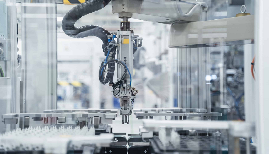
Malta, New York-based GlobalFoundries is a contract chipmaker, which means that it makes semiconductors for other companies based on those companies’ designs. Its fabs don’t use the latest manufacturing processes employed by the likes of Taiwan Semiconductor Manufacturing Co. Instead, GlobalFoundries relies on legacy technologies that trade off some performance for lower costs.
“As a strategic supplier of Qualcomm, GlobalFoundries shares our vision for strengthening U.S. chip production capacity,” said Qualcomm Inc. Chief Executive Officer Cristiano Amon. “This commitment from GlobalFoundries will help secure a resilient semiconductor supply chain to support the next wave of U.S. technology innovation.”
GlobalFoundries’ new $3 billion investment will go towards upgrading its manufacturing facilities in New York and Vermont. The Vermont plant makes chips based on gallium nitride, or GaN, a silicon alternative. The chipmaker detailed today that GaN technology will be a focus of the new investment.
An atom’s electrons orbit its nucleus at different distances. The difference between those distances is known as the bandgap. GaN has more than double the bandgap of silicon, which allows it to withstand significantly higher voltages. As a result, GaN chips are often used in electric vehicle chargers and power supplies, the components responsible for managing the flow of electricity inside servers.
Another key feature of the technology is its high switching speed. A GaN chip can turn its circuits on and off much faster than a silicon processor. The faster a chip’s switching mechanism, the less heat it generates, which helps reduce operating temperatures.
Besides GaN technology, GlobalFoundries also listed silicon photonics and packaging as priorities of its new investment plan.
Silicon photonics is the term for semiconductors that contain embedded optical components such as laser emitters. Such components are mainly used to power fiber-optic networks. The technology is also found in certain systems, including certain types of quantum computers that use light to carry out processing. GlobalFoundries makes silicon photonics chips for both use cases.
Packaging, meanwhile, is the technology used to link together multiple chips into a single integrated circuit. Earlier this year, GlobalFoundries opened a facility that will supply packaging for silicon photonics devices. The hub is located on the premises of the company’s flagship chip manufacturing campus in New York, where it’s currently building a new fab that will significantly boost its production capacity.
Support our mission to keep content open and free by engaging with theCUBE community. Join theCUBE’s Alumni Trust Network, where technology leaders connect, share intelligence and create opportunities.
Founded by tech visionaries John Furrier and Dave Vellante, SiliconANGLE Media has built a dynamic ecosystem of industry-leading digital media brands that reach 15+ million elite tech professionals. Our new proprietary theCUBE AI Video Cloud is breaking ground in audience interaction, leveraging theCUBEai.com neural network to help technology companies make data-driven decisions and stay at the forefront of industry conversations.