 INFRA
INFRA
INFRA
INFRA


INFRA

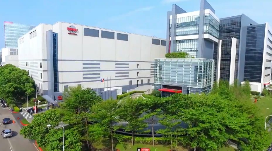
Taiwan Semiconductor Manufacturing Co. today posted second-quarter results that handily topped analyst expectations.
The company also announced plans to expand its fab complex in Arizona. TSMC intends to build at least four additional facilities at a cost of $100 billion, which will bring its total investment in the site to $265 billion.
The chipmaker’s profit surged 77% year-over-year in the second quarter, to 706.56 billion New Taiwan dollars, or about $21.89 billion. Analysts expected NT$632.64 billion. The profitability boost was partly driven by a 36% year-over-year top-line increase. TSMC closed the quarter with sales of $39.45 billion, a hair above the consensus estimate.
About two-thirds of the company’s revenue came from its high-performance computing segment, which includes data center chips. The segment is also the fastest growing of TMSC’s core businesses: Its revenue rose 20% on a quarter-over-quarter basis. Sales of smartphone chips, the company’s second-largest revenue source, dropped 4%.
TSMC’s advanced manufacturing technologies, nodes in the seven-nanometer range and below, accounted for 77% of wafer revenue. The company’s five-nanometer process is the most popular with a 33% share of sales. TSMC’s newest manufacturing technology, the two-nanometer N2 node it launched last year, currently accounts for only 2% of its revenue. But that number is set to increase significantly in the coming years.
Two of the four Arizona fabs that TSMC plans to build as part of its new $100 billion investment plan will use nodes in the two-nanometer range and below. They will operate alongside a third N2 fab that the company started building last year.
N2 is the first TSMC node to feature a gate-all-around transistor design. The design boosts power efficiency and provides chip engineers with more customization options than earlier architectures. Additionally, N2 uses tiny energy storage devices called MIM capacitors to optimize the flow of electricity in chips.
TSMC plans to offer multiple versions of its two-nanometer process. There’s a data center variant called N2X that uses more power than the standard edition and offers higher performance. In April, the company debuted an implementation dubbed N2A that is geared towards the auto sector.
The two other new plants that TSMC plans to build in Arizona will make advanced packaging components. Those are modules that can link together multiple silicon dies into a single processor. TSMC didn’t specify which of its advanced packaging products will be made at the fabs.
The company’s packaging portfolio is headlined by two technologies called SoIC and CoWoS. The former product makes it possible to link together multiple chiplets by stacking them atop one another. CoWoS, in turn, connects silicon dies by placing them side-by-side on a shared substrate. Earlier this year, TSMC previewed an upcoming CoWoS upgrade that will make it possible to link together 10 large compute dies and 20 HBM stacks.
The company is also developing multiple successors to its cutting-edge two-nanometer node. Next year, TSMC will launch a 1.6-nanometer node that places power delivery circuitry below transistors to boost chip efficiency. The technology is set to be followed by two processes dubbed A14 and A12.
TSMC will boost capital expenditures to support its engineering roadmap. The company disclosed today that it plans to spend between $60 billion and $64 billion in 2026, a significant increase from the $52 billion to $56 billion it projected before. TSMC also raised its full-year revenue growth guidance to just over 40%.
Support our mission to keep content open and free by engaging with theCUBE community. Join theCUBE’s Alumni Trust Network, where technology leaders connect, share intelligence and create opportunities.
Founded by tech visionaries John Furrier and Dave Vellante, SiliconANGLE Media has built a dynamic ecosystem of industry-leading digital media brands that reach 15+ million elite tech professionals. Our new proprietary theCUBE AI Video Cloud is breaking ground in audience interaction, leveraging theCUBEai.com neural network to help technology companies make data-driven decisions and stay at the forefront of industry conversations.