


 INFRA
INFRA
INFRA
INFRA
INFRA
Intel Corp. executives today detailed a new business vision for its foundry unit, freshly renamed Intel Foundry, and revealed the most advanced chip manufacturing process on the company’s technology roadmap.
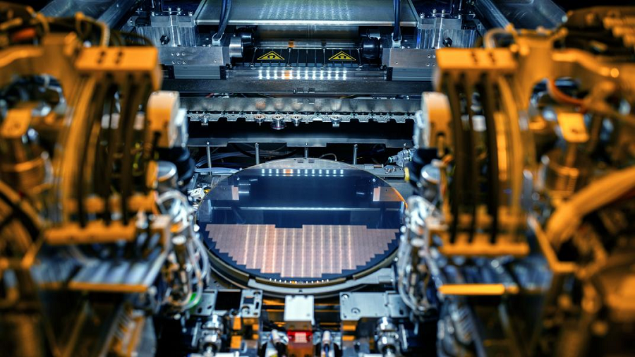
The process will be powered by High NA EUV machines from ASML Holdings NV. The machines, which are about the size of a double-decker bus and cost $350 million apiece, can produce the smallest transistor of any commercially available lithography system. ASML’s first-ever High NA EUV unit arrived at an Intel fab in Oregon late last year.
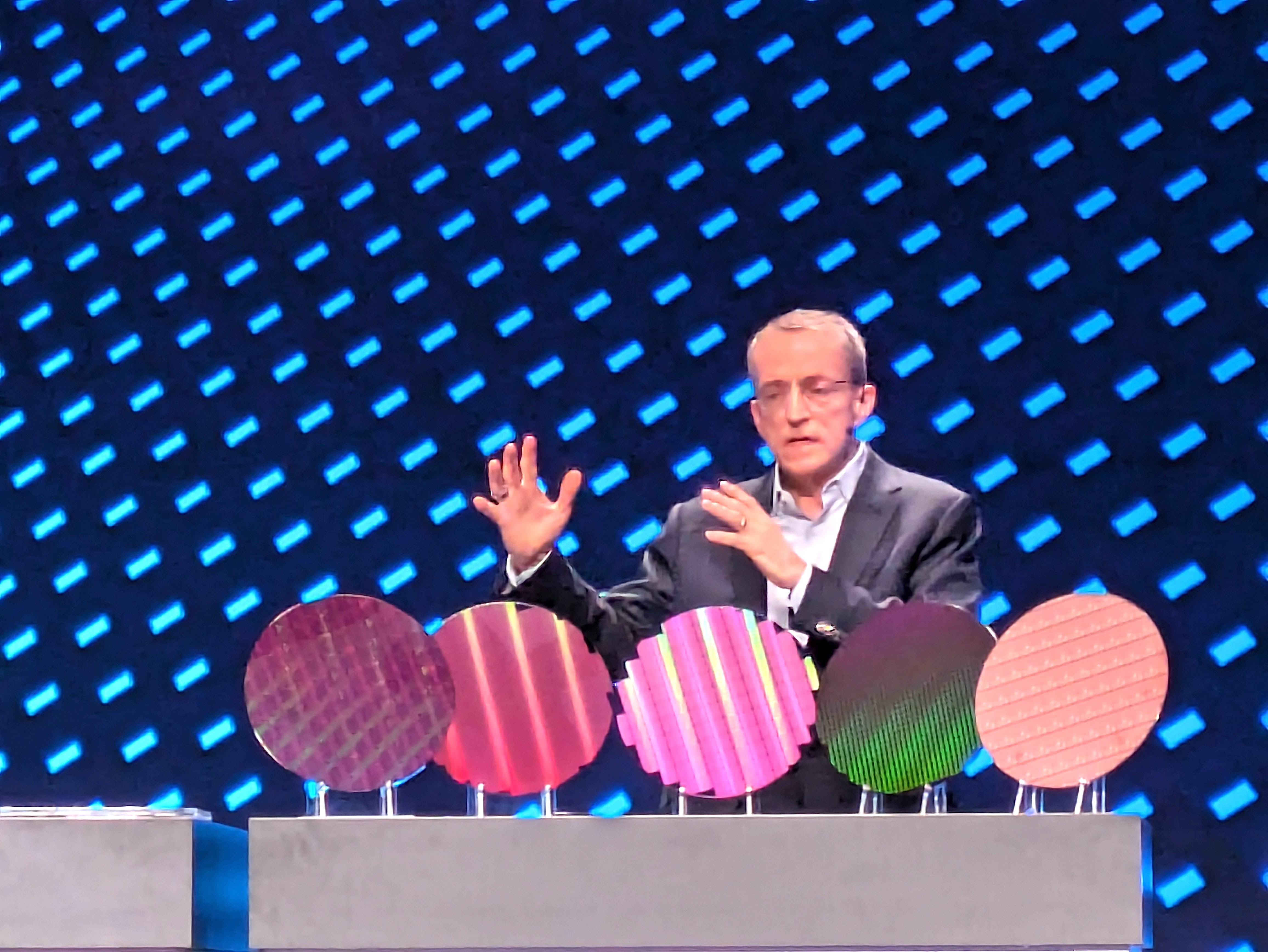
The chipmaker detailed its plans for Intel Foundry today at Foundry Direct Connect, its first-ever event dedicated to contract processor manufacturing. Alongside a keynote by Chief Executive Officer Pat Gelsinger (pictured), the conference featured remote appearances by U.S. Secretary of Commerce Gina Raimondo, Microsoft Corp. CEO Satya Nadella CEO and, due later today in person, OpenAI CEO Sam Altman. Executives from other major chip industry players such as Broadcom Inc. were in attendance as well.
Intel detailed that its foundry business has so far won chip production deals with a total lifetime value of more than $15 billion. At least one of those contracts, a deal to make an unspecified custom chip for Microsoft, will leverage the upcoming Intel 18A manufacturing process. This process will make transistors based on the gate-all-around design that Intel’s top rivals are currently also in the process of adopting.
“This is a renaming, a reorganization, a new organizational model,” Gelsinger said onstage. “A rebuilding of Intel.”
Until today, the gate-all-around Intel 18A node was the most advanced manufacturing process on the company’s publicly disclosed development roadmap. At Foundry Direct Connect this morning, the chip giant detailed an even more advanced process called Intel 14A. It’s expected to come online by 2027 and will use ASML’s $350 million High NA EUV machines to carve transistors into chips.
High NA EUV machines use a new type of optical component, known as an anamorphic mirror, to direct the laser beams they generate onto silicon wafers. The laser beams can carve transistors with a resolution of eight nanometers, a significant improvement over the 13.5-nanometer resolution offered by previous-generation machines. High NA EUV equipment is also expected to reduce processor defects and speed up chip production, which should likewise be conducive to Intel’s manufacturing plans.
The newer ASML machines operate on the same principle as the current-generation EUV equipment Intel uses in its plants. They work by vaporizing a small quantity of tin thousands of times per second to produce powerful laser beams. Most of the photons are absorbed by the optical components through which they pass on their way to the fab operator’s wafers, but the remaining light is still intense enough to produce high-accuracy transistors.
“We’re not done with Moore’s Law,” Gelsinger said. “Moore’s Law is alive and well.”
Alongside the Intel 14A reveal, the company today disclosed that it plans to offer some upcoming processes in multiple versions. One such version, which will be designated with the letter P, will offer 5% to 10% higher performance than the basic edition. Intel rival Taiwan Semiconductor Manufacturing Co. likewise offers some nodes in performance-optimized editions.
Intel is also planning a “T” flavor of some upcoming processes. The technology will provide support for through-silicon vias, tiny wires that make it possible to stack multiple chips atop one another to create one large, three-dimensional processor. Intel used through-silicon vias to build its GPU Max Series artificial intelligence accelerator, which combines 47 semiconductor modules with about 100 billion transistors into a single product.
“AI is profoundly transforming the world and how we think about technology and the silicon that powers it,” Gelsinger said. “This is creating an unprecedented opportunity for the world’s most innovative chip designers and for Intel Foundry, the world’s first systems foundry for the AI era.”
Engineers craft chip designs using a specialized type of application known as an electronic design automation, or EDA, tool. Today, Intel said a half-dozen EDA software makers will provide “tool qualification and IP readiness” to help customers design chips that can be made using the Intel 18A process. Cadence Design Systems Inc. is among the participants as are Synopsys Inc. and Ansys Corp., which are currently in the process of merging through a $35 billion acquisition.
In many cases, chip teams don’t start a new project from scratch but rather base their silicon on prepackaged blueprints from Arm Holdings plc. At Foundry Direct Connect today, Intel detailed that it’s teaming up with the British chip designer on an effort dubbed the Emerging Business Initiative. It will see the companies provide manufacturing support, financial assistance and other resources to startups developing Arm-based systems-on-chip.
“We are offering a world-class foundry, delivered from a resilient, more sustainable and secure source of supply, and complemented by unparalleled systems of chips capabilities,” said Stuart Pann, senior vice president of Intel Foundry. “Bringing these strengths together gives customers everything they need to engineer and deliver solutions for the most demanding applications.”
With reporting from Robert Hof
Support our mission to keep content open and free by engaging with theCUBE community. Join theCUBE’s Alumni Trust Network, where technology leaders connect, share intelligence and create opportunities.
Founded by tech visionaries John Furrier and Dave Vellante, SiliconANGLE Media has built a dynamic ecosystem of industry-leading digital media brands that reach 15+ million elite tech professionals. Our new proprietary theCUBE AI Video Cloud is breaking ground in audience interaction, leveraging theCUBEai.com neural network to help technology companies make data-driven decisions and stay at the forefront of industry conversations.