


 INFRA
INFRA
INFRA
INFRA
INFRA
Nearfield Instruments B.V., which specializes in producing advanced chip manufacturing equipment, revealed today it has gotten a massive $380 million capital injection.
The Dutch company’s Series D round was led by Fidelity Management & Research Company and saw participation from a host of well-known global investors, including Walden Catalyst Ventures, Temasek, Innovation Industries, M&G and Invest-NL. The Qatar Investment Authority joined the round as a new investor, while existing backers TNO Ventures and ING also participated.
The Rotterdam-based company said the round is the largest ever raised by any Dutch company, and brings its valuation to $1.6 billion, cementing its unicorn status.
Nearfield is trying to solve one of the most important, yet often overlooked challenges posed by the artificial intelligence boom: the difficulty of manufacturing the silicon processors that provide the brains of AI models. As new frontier models scale up in size and complexity, semiconductor manufacturers are being asked to deliver exponential gains in compute performance, while also reducing the energy consumption of these more advanced chips so they can process data faster without an exponential leap in cost.
To deliver these increasingly powerful processors, chipmakers have shrunk the size of their transistors to almost atomic levels while stacking them in complex, three-dimensional architectures. The goal is to squeeze more numbers of transistors onto silicon wafers to increase their computational power, but doing this isn’t easy. As chipmakers move onto more advanced manufacturing nodes such as gate-all-around and complementary field-effect transistor architectures, the fabrication process has become much more complex.
Now, one of the major bottlenecks is not the design process, but being able to inspect them properly during the manufacturing process. Even a slight imperfection can degrade the performance of a chip to the point where it’s essentially worthless, and if that happens too often, it can cripple production yields, increasing production costs to an unsustainable level.
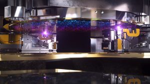
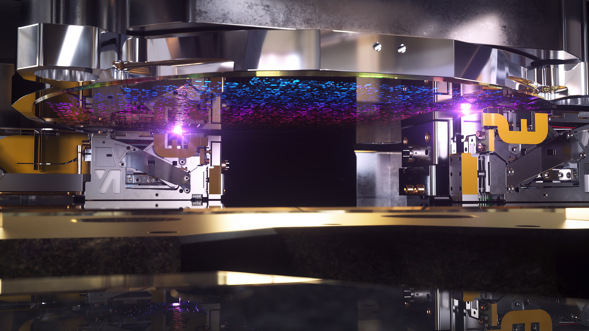
This is where Nearfield believes it can help. It’s a developer of advanced semiconductor 3D metrology and process control systems. Metrology is the intricate science of measuring the microscopic-sized structures that are etched onto silicon wafers. Chipmakers must have a way to ensure absolute precision, and that means being able to continuously monitor, adjust and perfect the manufacturing process to minimize defects.
Nearfield’s specialized equipment carries out high-throughput 3D scanning of wafers in order to measure these structures. Its tools provide visibility into the deep trenches and hidden layers within chips that utilize 3D stacking architectures, so that the depth, shape and other key dimensions can be measured accurately. These vital measurements enable chip fabs to identify flaws in real time, make the necessary adjustments to prevent them from reoccurring, and dramatically improve production yields.
Co-founder and Chief Executive Hamed Sadeghian said today’s round underscores the growing importance of his company in the global chipmaking supply chain. ‘We’re building a global technology company that’s here to stay, scale and lead,” he said. “It’s a defining moment in our journey and reflects the growing strategic importance of metrology and inspection in the era of AI-driven semiconductor innovation.”
The demands of AI models are forcing chipmakers to innovate at a much faster pace than ever before, and when their chip technologies improve at such a rate, they also have to make improvements to areas like quality control, said Holger Mueller of Constellation Research. “This is exactly what Nearfield is going to do after raising a respectable $380 million to enhance its capabilities,” the analyst said. “This is critical because metrology is becoming more challenging than ever as AI processors get smaller and smaller, and their architectural complexity increases. This will help Nearfield become more relevant and more global.”
Nearfield has laid out an aggressive roadmap to scale its operations and will use the capital from today’s round to accelerate technology innovation and expand its own production capacity so it can build enough of its inspection machines to meet the rising demand it’s seeing. It will also establish a number of Applications Centers of Excellence globally with the goal of expanding its collaborative research efforts with the world’s biggest semiconductor manufacturers.
Walden Catalyst Ventures’ Managing Partner Young Sohn said the shift to 3D chip architectures means Nearfield is poised to become a major player in the global semiconductor industry. “As the industry enters a critical new phase, advanced metrology and inspection will become essential enablers of the next generation of chip innovation,” he said.
Support our mission to keep content open and free by engaging with theCUBE community. Join theCUBE’s Alumni Trust Network, where technology leaders connect, share intelligence and create opportunities.
Founded by tech visionaries John Furrier and Dave Vellante, SiliconANGLE Media has built a dynamic ecosystem of industry-leading digital media brands that reach 15+ million elite tech professionals. Our new proprietary theCUBE AI Video Cloud is breaking ground in audience interaction, leveraging theCUBEai.com neural network to help technology companies make data-driven decisions and stay at the forefront of industry conversations.