


 INFRA
INFRA
INFRA
INFRA
INFRA
IBM Corp. today unveiled what it says is the world’s first sub-one-nanometer chip technology, a research breakthrough that it said will fuel the next 10 years of semiconductor development and pave the way to atomic-level chip design.
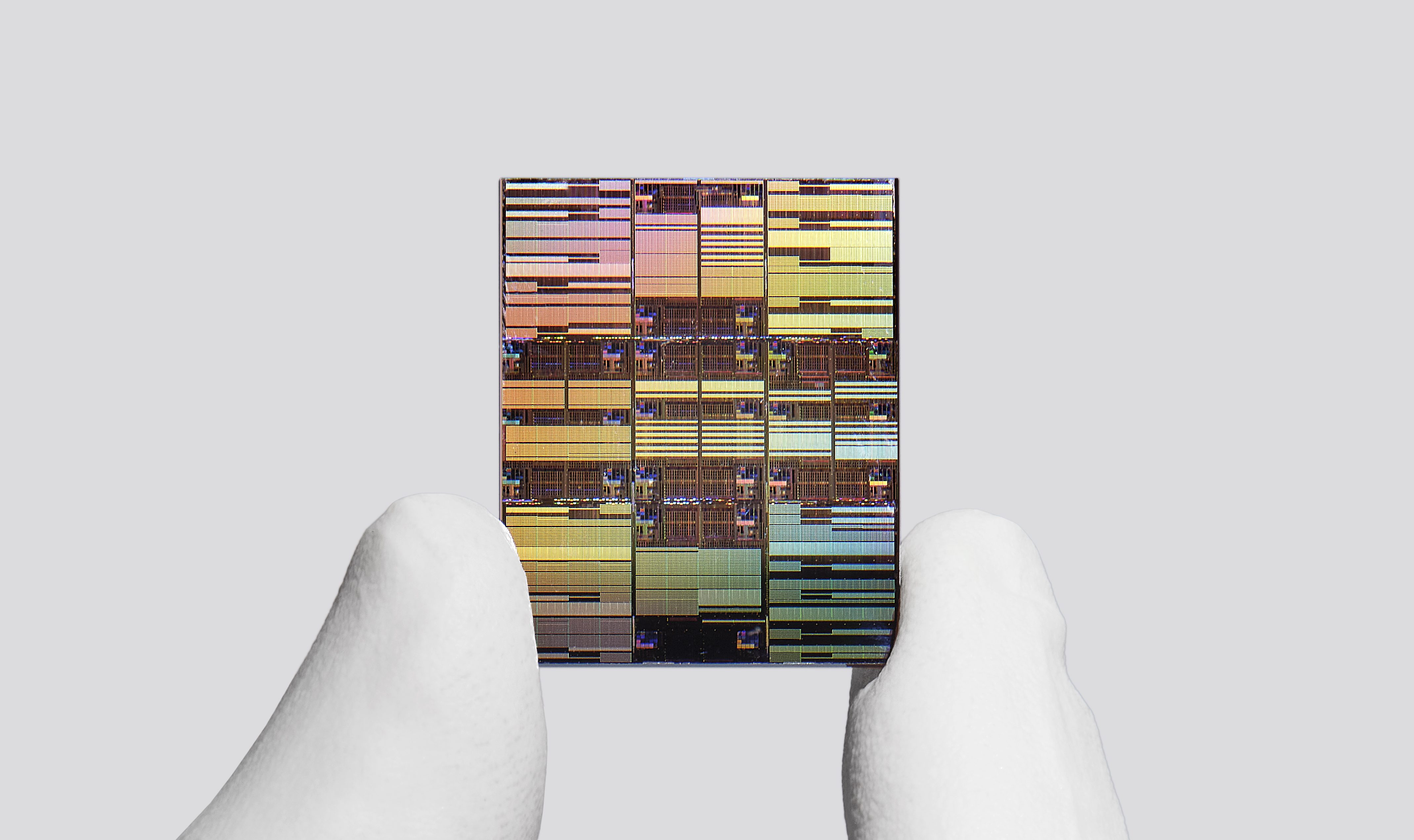
The new technology is based on a transistor architecture IBM calls nanostack, designed for the 0.7-nanometer, or seven-angstrom, node. IBM said the architecture can pack nearly 100 billion transistors onto a chip about the size of a fingernail (pictured), or nearly twice the density of the two-nanometer chip technology the company introduced in 2021.
IBM said the technology is projected to deliver up to 50% better performance and 70% greater energy efficiency compared with its two-nanometer node chips. The company also cited a 40% improvement in static random-access memory scaling, a development it said could be significant for artificial intelligence systems that need high-bandwidth, high-efficiency memory close to compute resources.
“It’s not just an incremental step, it’s a meaningful leap forward… pointing to a future where computing becomes significantly more powerful without a corresponding increase in energy,” said Jay Gambetta, director of IBM Research and an IBM Fellow.
Nanostack builds on nanosheet technology, a transistor architecture IBM helped pioneer that has become the basis for leading-edge chips. Nanosheet was the industry’s answer to the limits of fin field-effect transistors, the 3D transistor architecture used in modern microchips, so named for its raised, fin-like structure.
Nanosheet improved transistor channel control, reduced power leakage and enabled scaling into the three- and two-nanometer generations. Nanostack is IBM’s proposed next step beyond nanosheet, using vertical stacking to keep scaling going below 1nm. It adds a third dimension to chip scaling rather than relying solely on shrinking features across the wafer surface.
Such innovations have kept semiconductor technology moving beyond physical limits of miniaturization, said Huiming Bu, vice president of silicon technology research and development at IBM. “When something is coming to an end, it doesn’t mean the progress stops,” he said. “What it means is that we need a new paradigm.”
He said the semiconductor industry has largely scaled metal-oxide-semiconductor field-effect transistors in two dimensions since the transistor was invented in 1959. Nanostack’s vertical-stacking architecture allows designers to leverage the third dimension to increase density.
“This will be for the first time in our industry that we are able to stack and stagger transistors in a vertical direction,” Bu said.
An IBM research paper published last year describes nanostack as a sequentially stacked complementary metal-oxide-semiconductor architecture with flexible placement of top and bottom nanosheet channels, ultra-thin dielectric bonding and a thermally stable bottom transistor gate stack. IBM said it has demonstrated the ability to manufacture nanosheet-on-nanosheet CMOS transistors, including functional CMOS inverters and electrical characteristics comparable to or better than non-stacked nanosheet baselines.
The design allows the top and bottom transistors to be engineered separately and to use different materials for each layer. IBM said that flexibility could enable performance and power optimizations that are difficult in conventional transistor structures, where multiple components must be integrated on the same plane.
The architecture could apply across multiple chip categories, including CPUs. graphics processing units and mobile processors.
“This is a generic technology,” Bu said. “We expect this architecture to be used for multiple applications.”
The potential uses in artificial intelligence are likely to draw particular attention because power consumption has become a constraint on data center expansion. As AI models grow and inference demand increases, chipmakers are under pressure to improve performance without forcing proportional increases in power, cooling and infrastructure costs.
“Everyone demands more performance, but no one wants to pay for the bill for the power,” Bu said.
Gambetta said the SRAM scaling benefits are especially relevant because many AI chips rely heavily on on-chip memory to reduce data movement, which is one of the largest sources of energy consumption. More efficient SRAM designs could help increase cache capacity and reduce the need to move data between processors and external memory.
IBM cautioned that the technology is on a research-to-manufacturing path rather than a commercial product. The company said it expects the earliest adoption of nanostack at the sub-nanometer node to come within the next five years.
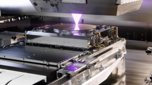
The work is being conducted at IBM’s semiconductor research facility in Albany, New York, where the company and its partners are also preparing to use High Numerical Aperture Extreme Ultraviolet Lithography, a next-generation chipmaking tool developed by ASML Holding N.V. IBM said High NA EUV will be important for future logic scaling and could also improve nanosheet technology before nanostack reaches production.
IBM said it’s currently working with partners including Japan’s Rapidus Corp. on two-nanometer manufacturing. Gambetta said IBM isn’t yet disclosing how it will commercialize nanostack, saying the company’s near-term focus remains helping partners scale nanosheet technology.
Support our mission to keep content open and free by engaging with theCUBE community. Join theCUBE’s Alumni Trust Network, where technology leaders connect, share intelligence and create opportunities.
Founded by tech visionaries John Furrier and Dave Vellante, SiliconANGLE Media has built a dynamic ecosystem of industry-leading digital media brands that reach 15+ million elite tech professionals. Our new proprietary theCUBE AI Video Cloud is breaking ground in audience interaction, leveraging theCUBEai.com neural network to help technology companies make data-driven decisions and stay at the forefront of industry conversations.