 EMERGING TECH
 EMERGING TECH
 EMERGING TECH
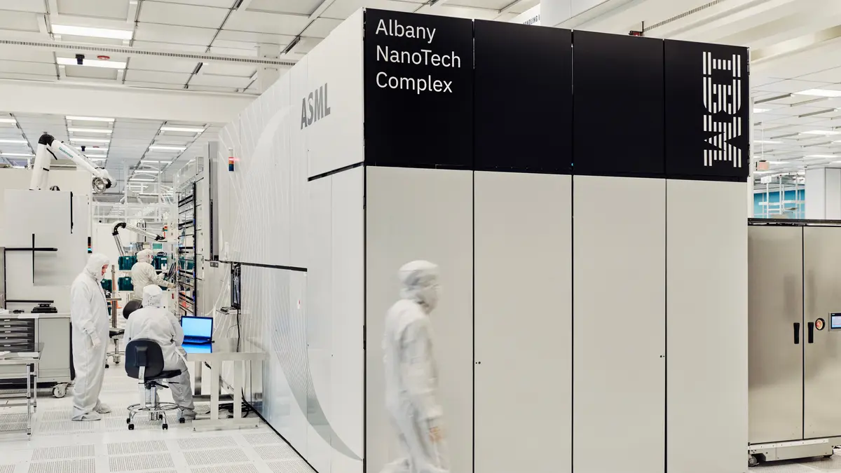
The state of New York, IBM Corp., Micron Technology Inc. and other organizations are teaming up to build a $10 billion semiconductor research lab in Albany.
The centerpiece of the facility will be a truck-sized machine called the Twinscan EXE:5200. Made by ASML Holding NV, the system is expected to become a cornerstone of the upcoming two-nanometer chip manufacturing process that the semiconductor industry is currently working to launch. IBM, Micron and other companies helping to build the new research lab in New York will use it to explore how chipmakers can make the most out of the Twinscan EXE:5200’s capabilities.
The facility will be located on the premises of the University of Albany’s Albany NanoTech Complex, where IBM already operates a research hub. NY CREATES, the nonprofit that operates the complex, will coordinate the construction process. The project is set to be backed by $1 billion in state funds and at least $9 billion worth of private investment.
Construction will begin in 2024 and is expected to complete within two years. Once it’s fully operational, the lab will have 50,000 square feet of clean room space, or space suitable for hosting semiconductor manufacturing gear. Besides IBM and Micron, the facility will also be used by chipmaking equipment suppliers Applied Materials Inc. and Tokyo Electron Ltd. as well as other organizations.
“The new High NA EUV Center at Albany NanoTech will secure a strong pipeline for semiconductor innovation, keeping New York State at the center of semiconductor expertise, accelerating the growth of the global chip industry and helping to meet manufacturing demand for new technologies such as generative AI,” said IBM Chief Executive Officer Arvind Krishna.
The Twinscale EXE:5200 system that will be installed in the facility reportedly costs more than $300 million. It’s the successor to the extreme ultraviolet lithography, or EUV, machines, made by Netherlands-based chipmaking equipment supplier ASML. The company’s EUV machines are used to make the fastest, most energy-efficient processors on the market.
The EXE:5200 works similarly to ASML’s current EUV systems: it vaporizes a small quantity of tin numerous times per second to produce a steady stream of laser pulses. Those laser pulses carve transistor-shaped patterns into silicon wafers, forming functioning circuits.
The key difference between the two ASML machine generations is their resolution. Current-generation EUV systems carve transistor patterns with a maximum accuracy of 13 nanometers. The EXE:5200 can achieve a much better resolution of 8 nanometers, which means it’s capable of manufacturing smaller, more power-efficient transistors.
Smaller transistors facilitate the creation of faster chips. In 2021, IBM demonstrated a proof-of-concept chip made using an experimental two-nanometer process. The company estimated that the technology could facilitate the creation of processors up to 45% faster or 75% more power-efficient than the most advanced silicon available on the market at the time.
IBM made the two-nanometer chip using a current-generation EUV machine. It’s possible to make two-nanometer processors using EUV gear, but not in a manner that lends itself to cost-effective mass production. The Twinscan EXE:5200 machine that will be installed in the new Albany chip research lab is expected to provide the key to efficient high-volume manufacturing.
An EUV machine requires three or four attempts to etch accurate two-nanometer transistors into a silicon wafer. The Twinscan EXE:5200 does so with only one pass, which means it’s capable of producing more processors in the same amount of time. That accelerated manufacturing pace not only increases the volume of two-nanometer processors a chipmaker can produce but also decreases costs.
Once online, the upcoming Albany chip lab will be the first and only publicly owned research hub in the U.S with a Twinscan EXE:5200. As of earlier this year, Intel Corp. was working to set up another such machine at its chip fab in Oregon. The company disclosed in October that it was planning to install its Twinscan EXE:5200 by year’s end.
Intel originally intended to use Twinscan EXE:5200 systems for an upcoming manufacturing process known as Intel 18A. The process implements a transistor design called the gate-all-around, or GAA, architecture that rival chipmakers are also adopting. Intel 18A was originally set to come online in 2025 but is now on track to begin mass production next year.
In September, the company revealed it no longer plans to mass-produce Intel 18A chips with EXE:5200 machines. Instead, it will only leverage the upcoming manufacturing process to test the machines and validate them for future use. The company’s mass-production plans for the EXE:5200 now center on a future manufacturing process called Intel Next that will launch after Intel 18A.
Support our mission to keep content open and free by engaging with theCUBE community. Join theCUBE’s Alumni Trust Network, where technology leaders connect, share intelligence and create opportunities.
Founded by tech visionaries John Furrier and Dave Vellante, SiliconANGLE Media has built a dynamic ecosystem of industry-leading digital media brands that reach 15+ million elite tech professionals. Our new proprietary theCUBE AI Video Cloud is breaking ground in audience interaction, leveraging theCUBEai.com neural network to help technology companies make data-driven decisions and stay at the forefront of industry conversations.