 APPS
APPS
 APPS
APPS
 APPS
APPS
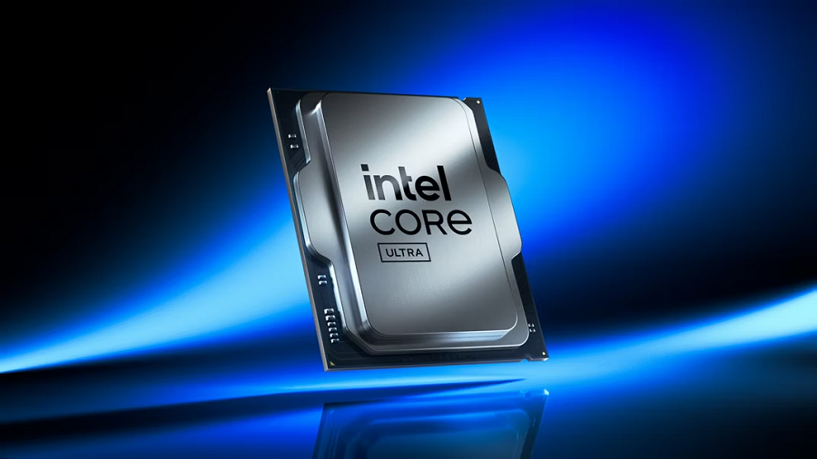
Intel Corp. today debuted a new desktop processor series, the Core Ultra 200S, that features five chips made using three-dimensional packaging technology.
The company is promising an up to 9% improvement in single-threaded performance compared with previous-generation silicon. For multithreaded workloads, the Core Ultra 200S offers a 14% speed boost. Power consumption is up to 58% lower depending on the workload.
The flagship chip in the Core Ultra 200S series is the Core Ultra 9 285K. It features eight performance-optimized cores with a maximum frequency of 5.6 gigahertz. There are also 16 efficiency-optimized cores that have a lower top speed, 4.6 gigahertz, but also use considerably less power.
The four other chips in the Core Ultra 200S series include 12 to 20 cores. They all share a common architecture with the flagship Core Ultra 9 285K.
The chips’ performance-optimized cores are based on a design that Intel calls Lion Cove. It’s 9% faster than the company’s previous-generation blueprint thanks partly to an improved cache. Intel has also upgraded the cores’ branch prediction mechanism, which carries out some calculations earlier than necessary to speed up processing.
The Core Ultra 200S series’ efficiency-optimized cores bring larger performance improvements. According to Intel, they perform calculations on floating point numbers up to 72% faster than previous-generation silicon. Tasks that involve integers are completed quicker as well.
The cores of a Core Ultra 200S processor are implemented on a chiplet that Intel refers to as the compute tile. It’s based on Taiwan Semiconductor Manufacturing Co. Ltd.’s N3B process. This is a specialized version of TSMC’s three-nanometer node that makes less extensive use of extreme ultraviolet lithography machines, which lowers production costs.
The compute tile is integrated with several other chiplets that are likewise made by TSMC. One chiplet contains a graphics processing unit that Intel describes as up to twice as fast as its previous accelerator. Another module features circuitry that manages the flow of data in and out of the processor, while a so-called SoC tile contains various auxiliary components.
All those modules sit on a base layer called the base tile. They’re linked together using a packaging technology called Foveros that makes it possible to place chiplets one atop another in a three-dimensional configuration.
Foveros uses tiny pieces of metal called microbumps to move data and power between the chiplets in a processor. The microbumps are located only a few dozen micrometers apart, which means up to 770 of them can be added to every square millimeter of a chip. Each square-millimeter patch of microbumps can move up to 160 gigabytes of data per second up and down a processor’s vertically stacked chiplets.
“The new Intel Core Ultra 200S series processors deliver on our goals to significantly cut power usage while retaining outstanding gaming performance and delivering leadership compute,” said Robert Hallock, vice president and general manager of AI and technical marketing at Intel’s client computing group. “The result is a cooler and quieter user experience.”
The Intel Core Ultra 200S series is set to become available later this month. The chips will ship with overclocking software, which allows users to boost the cores’ clock frequency beyond the factory-set maximum. It’s also possible to boost the speed of other components such as the interconnect that links together a Core Ultra 200S processor’s chiplets.
Support our mission to keep content open and free by engaging with theCUBE community. Join theCUBE’s Alumni Trust Network, where technology leaders connect, share intelligence and create opportunities.
Founded by tech visionaries John Furrier and Dave Vellante, SiliconANGLE Media has built a dynamic ecosystem of industry-leading digital media brands that reach 15+ million elite tech professionals. Our new proprietary theCUBE AI Video Cloud is breaking ground in audience interaction, leveraging theCUBEai.com neural network to help technology companies make data-driven decisions and stay at the forefront of industry conversations.