 INFRA
INFRA
INFRA
INFRA


INFRA

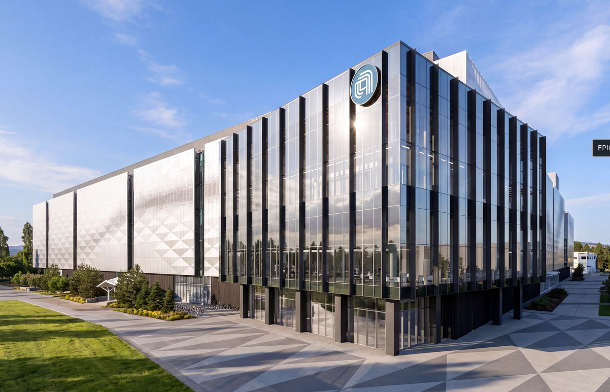
Semiconductor industry giant Applied Materials Inc. today opened the doors to its Equipment and Process Innovation and Commercialization Center, a massive new $5 billion facility in Silicon Valley that’s set to enable the next wave of breakthroughs in the commercial chipmaking industry.
The new EPIC Center, as it’s called, was built by Applied in order to provide the industry with a shared research and development facility, where some of the world’s smartest engineers can collaborate on new process manufacturing technologies.
The launch comes at a critical time. As artificial intelligence infrastructure buildouts continue to scale and frontier models become increasingly more powerful, the demands on compute have put the chipmaking industry under immense pressure.
Chip roadmaps have become more complex than ever as chipmakers race to innovate on more sophisticated processors that can accelerate compute performance and increase power savings beyond what current-generation silicon can do. Traditionally, the research and development process for new chip technologies could take up to a decade, but that won’t do in an industry that moves as quickly as AI.
Applied Chief Executive Gary Dickerson told the New York Post in an interview that the EPIC Center intends to accelerate these research processes as much as possible. The facility, which houses enough steel to build two Eiffel Towers, spans more than 600,000 square feet and is home to almost four acres of cleanroom space, all to support parallel, cross-industry R&D under one roof and shrink new innovation cycles.
“There are five to 10 key technologies that determine performance and yield [of semiconductors],” Dickerson told the Post. “It’s all about, how do we accelerate all of that? The goal here is to cut that whole cycle time at least 30%, improving the time to market. There’s enormous value in doing that.”
Inside, engineers from Applied plan to work collaboratively with their counterparts from some of the world’s biggest chipmakers on projects that aim to co-optimize new technologies such as 3D architectures, advanced packaging techniques, low-resistance wiring and hybrid bonding. The facility’s founding partners are a veritable who’s who of the chipmaking industry, including heavyweights such as Taiwan Semiconductor Manufacturing Co., Intel Corp., Samsung Electronics Co. Ltd., Micron Technology Inc. and SK hynix Inc.
Alongside them are a number of “innovation partners” that also will be helping out, including Broadcom Inc. and Advantest Corp., plus academic researchers from universities including Stanford University and the universities of California at Berkeley and Los Angeles.
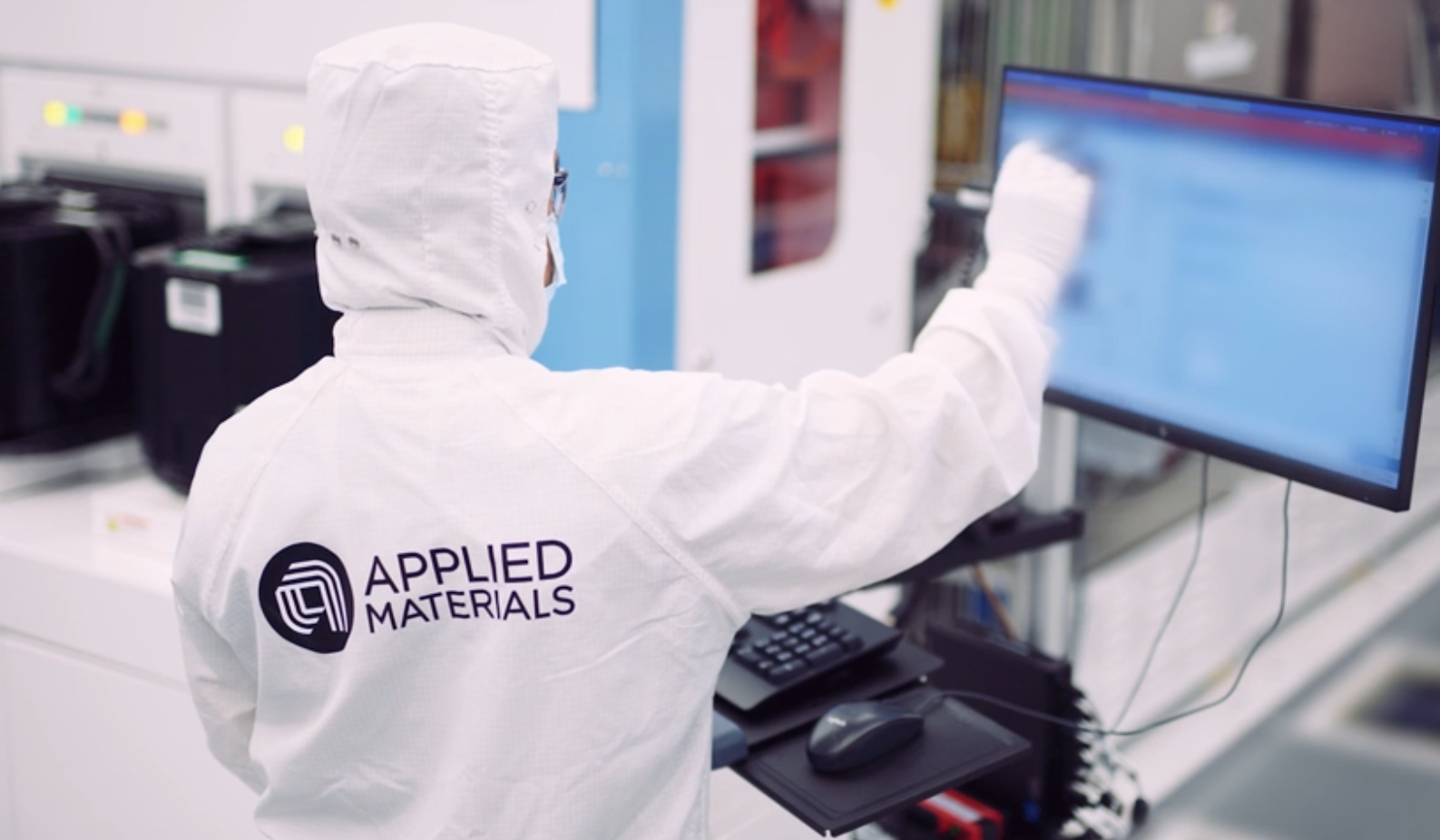
Intel CEO Lip-Bu Tan agreed with Dickerson that the chipmaking industry urgently needs to collaborate on transistors, interconnects and advanced packaging if it wants to take advantage of what he sees as a multitrillion-dollar opportunity for AI computing.
“We see a path to more than a trillion transistors in a package by 2030,” he said. “As architectures become more complex and R&D costs continue to rise, we need to move faster and work more closely with our equipment partners. EPIC gives our teams the opportunity to work side-by-side with Applied on materials and process innovation so we can accelerate development, improve R&D efficiency and bring new technologies to market faster.”
Applied’s Semiconductor Products Group President Dr. Prabu Raja said this collaborative approach to development will dramatically accelerate the process of commercializing new technologies.
“At today’s atomic-scale dimensions, many materials and materials interfaces behave in entirely new ways, and making them work at industry scale demands coordinated development and integrated solutions,” he explained. “EPIC is the only place where materials, process technology and equipment will be innovated in parallel, which increases the success rate of new materials and technologies. Because our customers’ own engineers help optimize the technology before it ever reaches their factory, what leaves EPIC arrives at the fab ready to ramp to high performance and high yield sooner.”
Dickerson told the Post that the EPIC Center could help researchers to compress new development lifecycles by at least 30%, and said doing this will be critical to easing the enormous energy demands that AI compute has placed on the world. “It’s absolutely essential,” he said. “You’re improving that energy-efficient computing many times versus where we’re at today. It’s many, many times better than where we’re at today.”
Dickerson declined to talk about any of the specific research projects currently underway at the EPIC Center, but he promised that some of the first breakthroughs will have major implications across healthcare, industrial production and education, as well as electronic devices such as smartphones and computers. “You’re going to see new consumer devices that go beyond the smartphone, that I have some visibility into, that will change human to human interaction and human-to-world interaction,” he said.
Support our mission to keep content open and free by engaging with theCUBE community. Join theCUBE’s Alumni Trust Network, where technology leaders connect, share intelligence and create opportunities.
Founded by tech visionaries John Furrier and Dave Vellante, SiliconANGLE Media has built a dynamic ecosystem of industry-leading digital media brands that reach 15+ million elite tech professionals. Our new proprietary theCUBE AI Video Cloud is breaking ground in audience interaction, leveraging theCUBEai.com neural network to help technology companies make data-driven decisions and stay at the forefront of industry conversations.