


 Graphene is a material that could greatly improve the world of high technology in the future. Isolated by Andre Geim and Konstantin Novoselov (Nobel Prize in 2010 for their work) in 2004, graphene is one of the major interests of mobile manufacturers today. Among the most recent developments include the work of the CNRS, the University of Lorraine and Synchrotron Soleil on graphene nanoribbons, or those of IBM Research that has managed to create the first radio chip functional with graphene transistors.
The problem is that nobody has so far managed to control its large-scale production, while steady progress on the design of silicon transistors made this quest less necessary.
It now seems that Samsung has found the key. The Korean manufacturer claims to have mastered the synthesis process to produce mass graphene. Samsung accomplished this breakthrough with the help of Sungkyungkwan University.
Graphene is more durable than steel and has high heat conductibility as well as flexibility, which makes it the perfect material for use in flexible displays, wearables and other next generation electronic devices. This means that the manufacture of thinner and flexible smartphones could be launched shortly along with smarter battery and other bendable wearable devices.
In a blog post, Samsung said through its partnership with Sungkyungkwan University’s School of Advanced Materials Science and Engineering, Samsung Advanced Institute of Technology (SAIT) uncovered a new method of growing large area, single crystal wafer scale graphene. Engineers around the world have invested heavily in research for the commercialization of graphene, but have faced many obstacles due to the challenges associated with it. In the past, researchers have found that multi-crystal synthesis – the process of synthesizing small graphene particles to produce large-area graphene – deteriorated the electric and mechanical properties of the material, limiting its application range and making it difficult to commercialize.
The new method developed by SAIT and Sungkyungkwan University synthesizes large-area graphene into a single crystal on a semiconductor, maintaining its electric and mechanical properties. The new method repeatedly synthesizes single crystal graphene on the current semiconductor wafer scale.
Why is this important?
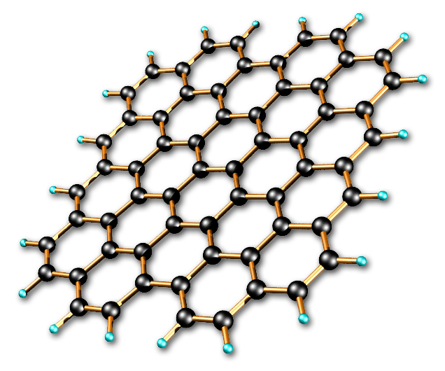
Graphene has a mobility of electrons 100 times that of silicon, the material most used currently in semiconductors. It is stronger than steel, has a high conductivity of heat and flexibility, making it the perfect material for flexible displays, clothing and connected objects and future generations of electronic devices.
Smartphone market is now maturing. Silicon is the predominant material utilized to build the individual electronic components within your favorite touchscreen enabled devices. But companies are now looking for the next big things like flexible, wearable devices to again boost mobile devices sale. As compared to silicon, graphene is said to have one hundred times the electron mobility. The use of graphene as a replacement for silicon would result in a faster, cooler and more efficient flow of electricity within our devices.
In addition, Graphene measures in at 0.33nm, that’s almost one million times thinner than a human hair, 97.7% transparent and is made of carbon. It has high heat conductivity as well. That means we can now see an ocean of new flexible, thinner and lighter devices powered by next generation of battery, which could charge itself instantly.
More flexible, conductive and can transmit more information than silicon, graphene could invade our smartphones and tablets in the future. Samsung now control the manufacturing technique and we expect to see the first products taking advantage of the expertise of the manufacturer.
“This is one of the most significant breakthroughs in graphene research in history,” said the laboratory leaders at SAIT’s Lab. “We expect this discovery to accelerate the commercialization of graphene, which could unlock the next era of consumer electronic technology.”
Flexible phones, super-fast computer
One could strengthen plastic with a graphene layer and render them electrically conductive. Moreover, graphene is suitable due to its transparency for the manufacture of screens and touch screens. The fact that the new material to play a prominent role in the development of electronic devices in future Samsung products.
Tech experts believe that Samsung will produce lighter, sturdier devices that would enable users to have complete control of their products without fear of breaking or snapping. The flexible devices could boost in the transition to larger, curved products that offer more viewing area.
Support our mission to keep content open and free by engaging with theCUBE community. Join theCUBE’s Alumni Trust Network, where technology leaders connect, share intelligence and create opportunities.
Founded by tech visionaries John Furrier and Dave Vellante, SiliconANGLE Media has built a dynamic ecosystem of industry-leading digital media brands that reach 15+ million elite tech professionals. Our new proprietary theCUBE AI Video Cloud is breaking ground in audience interaction, leveraging theCUBEai.com neural network to help technology companies make data-driven decisions and stay at the forefront of industry conversations.