


 INFRA
INFRA
INFRA
INFRA
INFRA
Intel Corp. has shared new technical details about Meteor Lake, an upcoming series of desktop and laptop processors that will feature chiplet technology.
Intel detailed the processor series today ahead of its presentation at Hot Chips, a major semiconductor industry event.
Intel historically implemented all the transistors that comprise a chip on a single piece of silicon. With the Meteor Lake series, the company will implement transistors not on a single piece of silicon but rather on multiple, smaller modules. This approach to chip design is known in the semiconductor industry as a chiplet architecture.
Each Meteor Lake processor will feature five different modules, or chiplets. The primary chiplet is a central processing unit that Intel will produce using its newest Intel 4 manufacturing process, which is also referred to as the company’s seven-nanometer process. According to the company, Intel 4 makes it possible to produce CPUs that can operate at up to 21.5% higher frequencies than previous-generation silicon using the same amount of electricity.
In Meteor Lake processors, the primary CPU chipset is integrated with three other chiplets that are made not by Intel but rather by Taiwan Semiconductor Manufacturing Co. Ltd. The three chiplets that TSMC will manufacture reportedly include a graphics processing unit, an I/O module for managing data input and output operations and a so-called SoC tile. Intel didn’t elaborate on what features the SoC tile provides.
With traditional semiconductor production techniques, it’s not possible to combine processing modules made by different companies in a single processor. Chiplet technology facilitates such configurations, which gives chipmakers such as Intel more flexibility in how they design their products.
Another benefit of the technology is that it can simplify manufacturing in certain respects. When the chiplets that comprise a processor are produced separately and linked together after manufacturing, hardware flaws become easier to manage. If one of the chiplets contains a flaw, the others can still be used.
The CPU, GPU, I/O module and SoC tile in Meteor Lake are all placed atop another, fifth chiplet in a three-dimensional configuration. That fifth chiplet reportedly doesn’t contain any logic circuits, or circuits capable of performing computations. It’s manufactured by Intel using its low-cost 22FFL chip fabrication process.
Placing chips atop one another in a three-dimensional configuration has several major advantages. Two processors placed atop one another have a smaller area than two processors placed next two each other, which is beneficial for compact devices such as laptops. Moreover, stacking chips enables data to travel faster between transistors under certain conditions, which can speed up processing.
Intel is using an internally developed technology known as Foveros to place Meteor Lake’s four main chiplets on the fifth, 22FFL-based chiplet that serves as the processor series’ foundation. Intel already implemented Foveros once before in a chip lineup called Lakefield that it discontinued in 2021. However, Meteor Lake is the first example of Intel using the technology to power a processor series that it will manufacture in large volumes.
The first Meteor Lake chips are expected to make their debut next year.
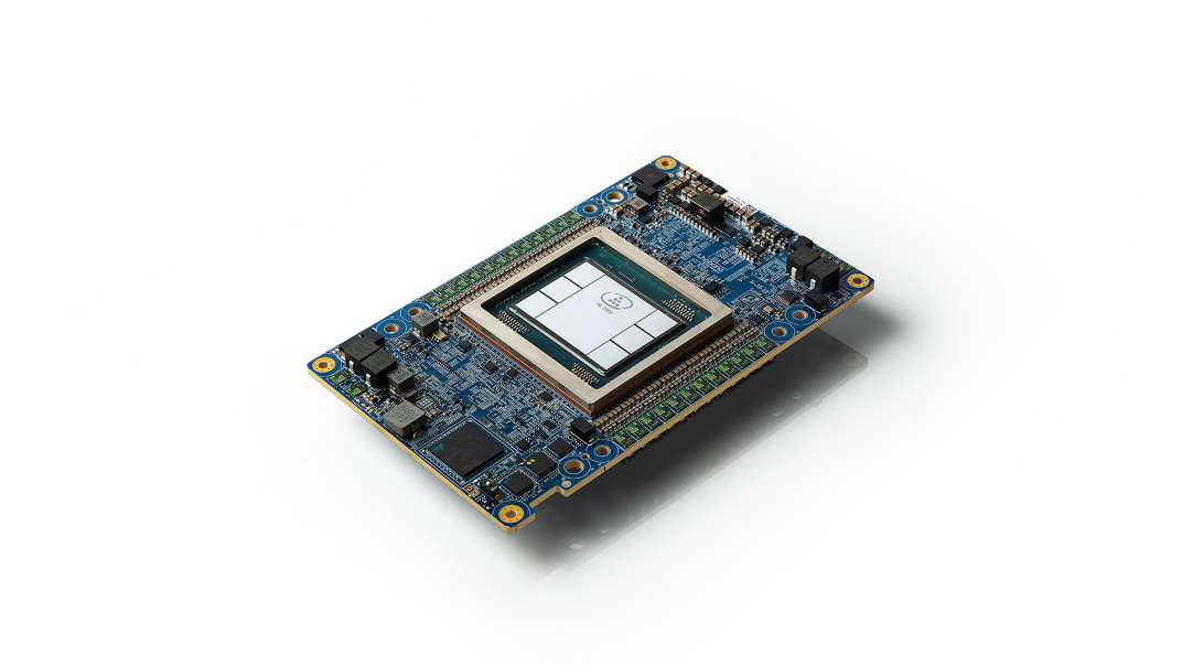
In addition to using Foveros to power laptop and desktop processors, Intel plans to bring the technology to the data data center market. The company last year debuted a Foveros-powered chip dubbed Ponte Vecchio that is optimized for machine learning workloads. The chip comprises 47 different chiplets made using five different manufacturing processes.
Across its various components, Ponte Vecchio features a total of 100 billion transistors. That’s nearly double the number of transistors in Nvidia Corp.’s flagship A100 data center graphics card. According to Intel, early Ponte Vecchio prototypes have demonstrated the ability to reach speeds of 45 teraflops, which equals 45 trillion computing operations per second.
Support our mission to keep content open and free by engaging with theCUBE community. Join theCUBE’s Alumni Trust Network, where technology leaders connect, share intelligence and create opportunities.
Founded by tech visionaries John Furrier and Dave Vellante, SiliconANGLE Media has built a dynamic ecosystem of industry-leading digital media brands that reach 15+ million elite tech professionals. Our new proprietary theCUBE AI Video Cloud is breaking ground in audience interaction, leveraging theCUBEai.com neural network to help technology companies make data-driven decisions and stay at the forefront of industry conversations.