 INFRA
INFRA
INFRA
INFRA








INFRA

Singapore-based startup Nexstrom Pte. Ltd. said today it has raised $12 million in seed funding to drag the chipmaking industry into the “post-silicon era” by commercializing its proprietary wafer-scale platform for 2D semiconductor materials.
Today’s round was led by Xora Innovation and saw participation from SEEDS and Foothill Ventures, bringing the startup’s total amount raised to $15 million so far. The money will help it toward its goal of becoming the first company in the world to mass-produce 12-inch 2D semiconductor wafers for a new generation of computer chips that abandon traditional silicon.
Nexstrom argues that a new kind of wafer is urgently needed by chipmakers. The rise of artificial intelligence models has fueled the desire for increasingly more powerful and energy-efficient chips, but the physical limitations of silicon have prevented that from happening, so far.
The problem is that it’s just not possible to continue shrinking the size of the microscopic channels etched into silicon wafers. Go any smaller and the electrons will start leaking, resulting in substantial power loss and inefficient computing. And that’s not feasible at a time when enterprises are putting together massive clusters of extremely powerful processors to train and run advanced AI models.
Alternatives to silicon do exist, and one of the most promising is a single-crystal 2D substrate made out of transition metal dichalcogenide materials. They consist of atomically thin crystals that can conduct electricity extremely efficiently at sub-nanometer scales. Because they’re so incredibly thin, they enable more precise electron control at the transistor level, supporting more efficient computing operations with reduced energy loss.
Notably, they eliminate interface flaws such as “micro-voids” to allow seamless control of transistor gates and reduce the leakage of electrical current. By swapping out the silicon in favor of these single-crystal 2D materials, it should be possible to develop chips with minute transistors beyond the sub-1 nanometer level.
Chipmakers have been aware of this technology for some time, said Nexstrom co-founder and Chief Scientist Lance Li, but until now, no one has come up with a feasible way to manufacture these wafers at a commercial scale. “For years, the challenge has not been demonstrating the promise of 2D materials, but manufacturing them at the scale and quality advanced foundries require,” Li explained.
Nexstrom’s mission is to change this, and it claims to have developed the first platform in the world that’s capable of growing single-crystal 2D semiconductor materials in the vast quantities the chipmaking industry requires. Until now, researchers have only been able to develop very small samples of the materials in laboratories, and their methods would require a complete overhaul of existing foundry systems, which means they’re just not feasible.
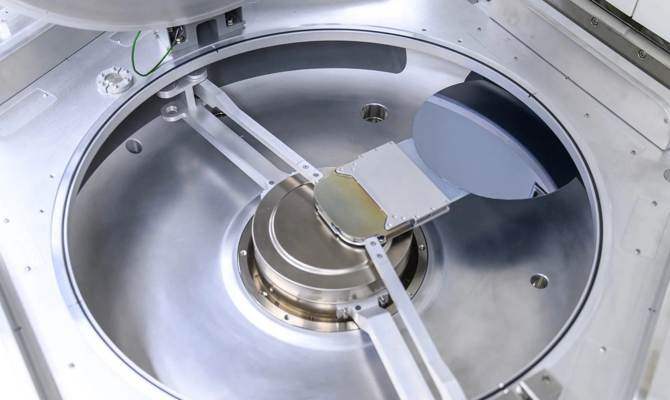
To get around this, Nexstrom integrates its proprietary chemical vapor deposition hardware with a novel process technology and wafer-scale 2D material growth directly into existing foundry workflows. By using specialized chemistry, it says it can continuously grow 12-inch single-crystal 2D wafers that are ready for mass production of more advanced chips, paving the way for the post-silicon era of computing
Dr. Philip Wong, a Stanford University professor who advises Nexstrom’s board, said 2D semiconductor materials are already on the roadmaps of the world’s biggest semiconductor firms, but they’re still waiting for a way to produce the materials at scale. “The industry needs high-quality, uniform 2D materials on 300 millimeter substrates, and solving that materials bottleneck is exactly where Nexstrom is focused,” he said.
Support our mission to keep content open and free by engaging with theCUBE community. Join theCUBE’s Alumni Trust Network, where technology leaders connect, share intelligence and create opportunities.
Founded by tech visionaries John Furrier and Dave Vellante, SiliconANGLE Media has built a dynamic ecosystem of industry-leading digital media brands that reach 15+ million elite tech professionals. Our new proprietary theCUBE AI Video Cloud is breaking ground in audience interaction, leveraging theCUBEai.com neural network to help technology companies make data-driven decisions and stay at the forefront of industry conversations.